ps. I wonder if you used gimp to get the picture in perspective
I used photoshop but you can do the same thing with gimp, in PS it's called "Perspective Crop Tool"
Follow along with the video below to see how to install our site as a web app on your home screen.
Note: This feature may not be available in some browsers.
ps. I wonder if you used gimp to get the picture in perspective
That is all jazz,.
Sorry but the charge of the proof is on the original poster. Compute is useful whether you have discrete or integrated GPU. Now if you know a game that can't run on PC if the CPU is not an APUs I will start to consider reconsidering my pov.heterogeneous computing
Has it been shown that there has been very little value add for HUMA and heterogeneous computing in general for these consoles ??
You could also do it with the 6 pin atx power connector on the board visible in the uncroped image. I don't have a measuring tape with me but just incase those memory modules are a different size for whatever reason for some weird reason you could also base measurements off that.Second attempt and an image
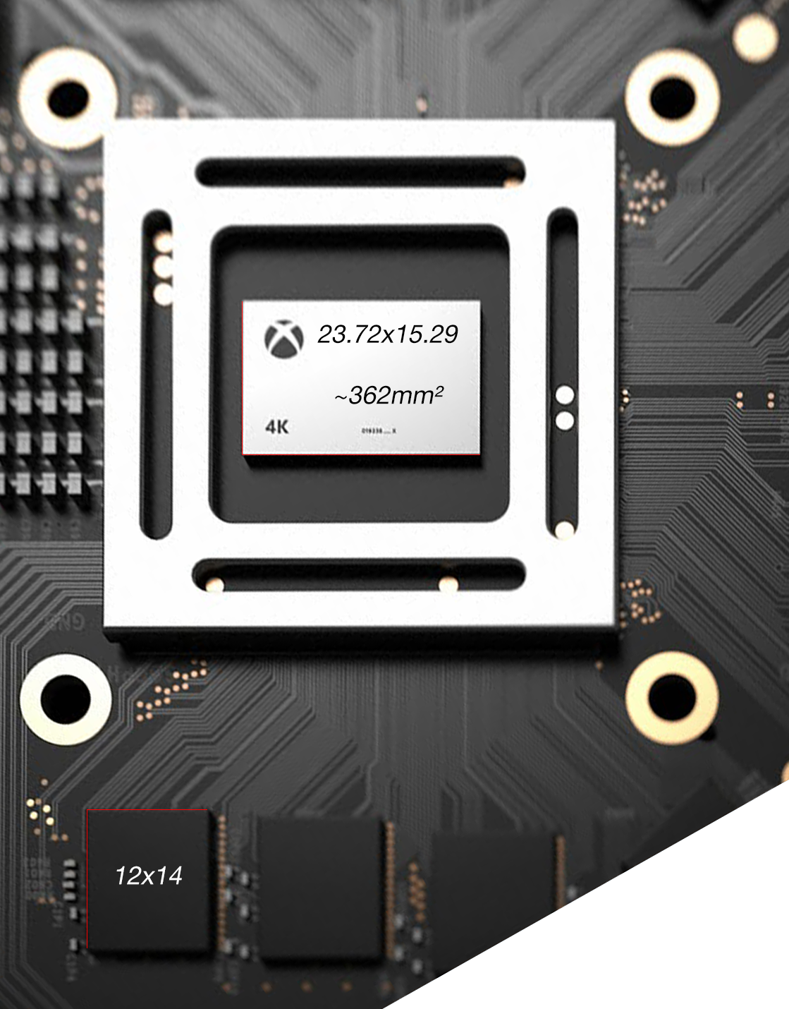
Non rounded numbers:
Height: 15.298245614035087719298245614035
Width: 23.719298245614035087719298245614
Die size: 362.86365035395506309633733456448
Actually pretty similar to X1 in terms of size if this is correct, which i'm not sure about as i'm hardly an expert in measuring dies
Math logic behind the measurement
- Draw line over memory module width (which according to micron is 12mm)
- Measure how many pixels on that line -> 12mm line = 171 pixels
- Draw lines for width and height on the die
- Measure pixels of each line in the actual die -> (#pixels/171)x12 = mm of each respective line on the die
- Multiply -> Profit
Just to test, used the exact same method for this (GM200): https://www.techpowerup.com/reviews/NVIDIA/GeForce_GTX_980_Ti/images/front_full.jpg
And the total die size came up to 600.49690695619239994950132559021, reported nvidia die size is 601mm² so i guess that's pretty close")
Polaris 10 is supposed to work at it's boost clocks on everything but the furmark & coBase clock of the 480 is 1080 mHz, iirc. Boost clocks aren't so useful in looking at what might translate to console land, at least traditionally.
Devs on a console could also push GPU utilization to the limit.Polaris 10 is supposed to work at it's boost clocks on everything but the furmark & co
Polaris 10 is supposed to work at it's boost clocks on everything but the furmark & co
On the bottom left corner I count 14 balanced lines (8 left, 6 more on the bottom). Smells like high bitrate interfaces like pcie, maybe there are 2 more lines hidden, for a total of 16.
I'm not rumor-mongering, I swear!
I'm not sure it has anything to do with size, it has more to with costs and added value. As CPU have gone tinier the manufacturers have started to integrate iGP into their CPU. Performances of those GPU have never really much more than a marketing bullet point (especially for AMD) and it helped cleaning the mobo, made sure any computer has some level of graphic acceleration. Recently they prove competent enough to drive some non demanding games but no gamers (with reasonable financial means) is fine with just that. On the mobile SOC, it is pretty much the same, performance (3D) are an after though compare to optimizing price (and footprint). CPU and GPU are different in many ways, till those recent huge steps in resolution the different between the size of the RAM and the V-ram was pretty massive, it is reduced now. GPU works pretty consistently, power usage varies but I would think less than a CPU, the turbo is lesser the GPU run slower. CPU is more of the "bursty" type,when the architecture the jump in turbo frequency can be a lot more significant. I see this a tough mariage i you put then on the same chip: the GPU is likely to eat the thermal/power room that the CPU might want to hit during its burst.If you go past a certain size, you might get more bang for your money with separate dies for CPU and GPU
I'm not sure about that, the cost overhead in cost of the whole memory set-up is also quite consistent and might spice up the bill significantly. Jaguar seems to be sucking bandwidth out of straw cheap DDR3 would have done the job. Completely down the road they could have mapped the system to a SOC with UMA and optimize completely for cost as technology would have caught up to speed with the original system.While more expensive in the long run, it might cut down time to market, cut down R&D needed for a more customized part, and then you just dump it and release a new system after a few years.
Microsoft could be working with Valve on Project Scorpio, according to TIME magazine.
http://time.com/4369910/xbox-one-s-project-scorpio-microsoft-e3-2016/
I’m not probably supposed to say this, but I sat down before this show with the leaders of Valve, and I showed them Scorpio and what we’re doing . . . Valve and Steam specifically is a massive part of the PC gaming community today, it’s growing like crazy, it will continue to grow. I think it’s got a long, great future ahead of it. I think as the platform holder of Windows, I think there are things we should be doing to make Windows 10 a great gaming experience. Valve applauds us. As [Valve co-founder] Gabe [Newell] says, there are going to be areas where we compete and areas where we cooperate and in the end of both of those are good for gamers.
I want to build a store, and people can look at that and say, you focusing on Windows Store is competition for Steam, I kind of laugh right now when I look at the numbers and people say I’m competitive with Steam at all, but we’re selling our first-party content.
Sure, but in a way I’d prefer if you didn’t call it a portable Xbox, because it’s a Razer. I think of Xbox as the service, and your content library, and you’re bringing Xbox to Razer. I’m not trying to turn PCs into consoles either.
PS4 neo gpu is supposedly clocked at 911MHz. So I'm thinking 52CU@900MHz for Scorpio.Something just struck me as I was sitting here thinking about the potential for the XBO-T to have a 384 bit memory bus.
If we compare it to Polaris 11 (Rx460) there's some interesting things that happen. Polaris 11 (Rx 460) in base configuration is over 2 TFLOPs (under 1 GHz for 2.0 TFLOPs and over 1.2 GHz for 2.5 TFLOPs), 128 bit memory interface with ~112 GB/s bandwidth. It has 16 CU's compared to Polaris 10's 36 CUs (for the Rx480).
If you triple Polaris 11's configuration and target less than =< 1 GHZ you end up with a 6 TFLOP configuration with a 384 bit memory interface and bandwidth that's probably right at 320 GB/s (basically everything clocked lower than Rx 460).
So, if we assume Vega is just a slight evolution of Polaris. I can totally see a 48 CU Polaris/Vega configuration with 384 bit memory interface clocked at =< 1 GHz.
Hmmm, another thought, would it be possible to have a 192 bit interface with faster memory to hit 320 GB/s? For instance, imagine if the lower end Vega card is going to be using GDDR5x with a 256 bit memory bus. Instead of XBO-T using something akin to 3x Polaris 11, perhaps it's 3/4 of the lower Vega variant?
Regards,
SB
PS4 neo gpu is supposedly clocked at 911MHz. So I'm thinking 52CU@900MHz for Scorpio.
I'm going to say 56CU@850 at least because MS will want to comfortably reach their performance metrics without pushing the APU to it's limits. I doubt very seriously if we'll see 900Mhz, Microsoft probably still has RROD nightmares. They want a quiet, cool experience, so they're not going to risk it.