predict how actual Xbox Next will differ from leaked specs

Status
Not open for further replies.
DaveBaumann said:
Yes, Vince, again you explain the obvious – but that still doesn’t mean that SI concur with the 45nm measurement, their statement just says that they agree that their initial explanation for the measurement differences was not the case and they still have measurement difference between SI and chipworks.

If it's obvious why do you post it as you did (namely wrong)? Look, they have failed to explain how several 45nm logic gates were produced. They claim it's a 130nm fabbed part, the burden is on them and they have NO explination of how Chipworks SEM can exist given their previous statements other than to reiterate them. Dave, this isn't a good position to be in, I have visual proof, 'you' (figuratively) dont.

DaveBaumann said:
They don’t have to be fabricated. There could have been measurement issues or how do we know that the chip they took the 45nm measurement from is indicative of a normal chip? Could this be an anomaly that may have caused issues in a fully functional chip?

No, both samples were taken out of production PSX's that they aquired after the launch in Japan. And it's not a measurement issue Dave, come on already. William of Ockham would kill you, and you guys say I'm bad.

DaveBaumann said:
It’s a discussion because there are contradictory evidences out there – one company has consistently said one thing (and still does) and another says something else (and I would like to know why the TOC for their own detailed analysis specifically highlights gate lengths that are inline with the SI).

The problem is that only one side (Sony, Chipworks and mine) is self-conistent. SI can't explain how the 45nm tranistsors were formed, nor can they disprove it. The transistors match what Sony and Toshiba claim for CMOS4 and fit the given data points, including die area. SI is the outlier...
 
If it's obvious when why do you post it as you did (namely wrong)? Look, they have failed to explain how several 45nm logic gates were produced.

The entire article was about the measurement processes, not the actual existence of the gates. They failed to explain how chipworks measured 45nm gates, not failed to explain how 45nm gates were produced.

Dave, this isn't a good position to be in, I have visual proof, 'you' (figuratively) dont.

Visual proof that there is some contention over between the company that took it and another that opposes it.

No, both samples were taken out of production PSX's that they aquired after the launch in Japan.

Can you point me to where it states that for the initial Chipworks release?

The problem is that only one side (Sony, Chipworks and mine) is self-conistent.

And why don’t Chipworks reference that in the TOC of their detailed analysis, only 65-70nm gate lengths? And, despite the roadmap you highlighted, Sony also appears to classify processes with transistor gate lengths of 70nm as 90nm, at least in the case of EDRAM, as witnessed by their ASC9 documentation.
 
DaveBaumann said:
And why don’t Chipworks reference that in the TOC of their detailed analysis, only 65-70nm gate lengths?

Didn't I post that gate length is only one of indicators of the process actually used? Check out this UMC's case -

http://www.chipworks.com/news/2004_UMC90nmProcess.asp

CHIPWORKS SEES UMC'S DIFFERENT APPROACH TO 90NM TECHNOLOGY. IS IT 90NM?

OTTAWA, CANADA, May 25th, 2004 - Chipworks Inc. ("Chipworks") the standard setting supplier of reverse engineering services, announced today that they are analyzing the Xilinx XC3S200 Spartan-3 FPGA. Findings indicate a discrepancy in reported process techniques.

Xilinx publicized their move to 90nm technology over a year ago, stating that the Spartan-3 product would be made in both the IBM and UMC foundries on 300 mm wafers. The device analyzed matches UMC's publicity and previous product investigated by Chipworks. It uses seven layers of copper, and one aluminum layer. Xilinx is using the 90nm technology to drive their target pricing down to under $12 for a one-million-gate FPGA and $2.95 for a 50,000 gate FPGA (approximately 17,000 and 1,700 logic cells respectively).

According to Dick James, a senior technology analyst for Chipworks, "we found transistor gate lengths less than 70nm, and a metal 1 (M1) pitch of ~250nm. While these do not meet the letter of the ITRS (International Technology Roadmap for Semiconductors) definition of 90nm feature sizes, they are in the range of 90nm processes announced by other companies. For example, Chipworks measured Texas Instruments' M1 pitch as 300nm and gate length as 48nm, and Intel's M1 pitch is 230nm and gate length is 45nm. ITRS sets the dimensions at 214nm and 37nm, respectively."

UMC's different and more conservative approach for the Xilinx chip lies in the dielectric layers used in the interconnect structure. SIMS analysis shows that the intermetal dielectrics (IMDs) are FSG (fluoro-silicate glass), with undoped glass at the top level. The copper metal is dual damascene, and no trench etch-stop layers have been used, therefore minimizing the effective k-value of the combined dielectric and metal-cap layers.

James stated, "this is the first part that Chipworks has seen that is claimed to be 90nm and is still using only the FSG that is universal in 130nm processes. Other 90nm technologies from Intel, Texas Instruments and Sony/Toshiba have all used low-k at the critical metal levels. Consequently, the question is - can we classify this as a 90-nm part, or is it a shrunk 130nm device?"

UMC's publicity for their 90nm L90 process details the M1 pitch as 240nm, and the gate length as 70nm, and shows the IMD as FSG at the upper metal layers, with low-k (k~2.7) at the lower levels. Reported press indicates that UMC is planning to use Novellus' Coral carbon-doped oxide as their low-k material. So the part meets the published dimensions for 90nm, but not the structural details.

From Xilinx's perspective, UMC has presumably met the performance specifications for the XC3S200 - our sample is the standard speed product. The major advantage from 90-nm processing is the reduction in die size, and therefore cost - there are over twice as many die per wafer, compared with the equivalent product in 130nm technology.

The Spartan product is Xilinx' low-cost FPGA series, where the emphasis is on the performance/price ratio, targeted at the widest range of consumer applications. The nature of the IMD will not affect the die size, so as long as the device meets the performance requirements, it is not relevant - unless FSG/90-nm is cheaper than low-k/90-nm. It may in fact be cheaper, since FSG is a much more mature process.

Chipworks' findings for this device will be available in an upcoming structural analysis report, so that process engineers can examine this different approach to nanometer silicon. The report will also include an overview, package and die photos, process, transistor, materials and dielectric analysis, as well as critical die dimensions.
 
Didn't I post that gate length is only one of indicators of the process actually used? Check out this UMC's case

Again, I'm not interested in the definition(s) at this point, I'm merely questioning the gate lengths. (But, as an aside, SI were also saying the metal pitch of the EE+GS was closer to that used one 130nm processes)
 
DaveBaumann said:
Didn't I post that gate length is only one of indicators of the process actually used? Check out this UMC's case

Again, I'm not interested in the definition(s) at this point, I'm merely questioning the gate lengths. (But, as an aside, SI were also saying the metal pitch of the EE+GS was closer to that used one 130nm processes)

Well, what I'd like to put emphasis on in the UMC's case is this; UMC's 90nm chip has 70nm gate length or less (so probably average 70nm) and is still in the criteria of 90nm, according to Chipworks. What's your problem? :rolleyes:
 
Again, not that this is the point that I'm trying to establish, but the last thing on that UMC report that relates to Chipworks appears to be not a statement of declaration, but an unanswered question - [Chipworks] : "Consequently, the question is - can we classify this as a 90-nm part, or is it a shrunk 130nm device?"
 
DaveBaumann said:
Again, not that this is the point that I'm trying to establish, but the last thing on that UMC report that relates to Chipworks appears to be not a statement of declaration, but an unanswered question - [Chipworks] : "Consequently, the question is - can we classify this as a 90-nm part, or is it a shrunk 130nm device?"

Have you read all the above story about UMC including low-k use etc?
 
Errr, yes, have you?

First paragraph: “Chipworks Inc. ("Chipworks") the standard setting supplier of reverse engineering services, announced today that they are analyzing the Xilinx XC3S200 Spartan-3 FPGA. Findings indicate a discrepancy in reported process techniques.â€￾

Third paragraph they stay that their findings are in the ranges of other reported companies (although much larger metal pitches and gate lengths than Intel, and smaller metal pitch that TI but larger gate length), but the final paragraph concerning chipworks they are not making a declaration that they believe this is a 90nm process, instead leaving it open questioning whether it is 90nm or shrunk 130nm (much like TSMC's 110nm process, that is also non-low-k).
 
Dave: It's odd the IEDM 2002 paper of Sony/Toshiba brings 70nm gate length instead of 45nm in discussing the 90nm process technology.

Chipworks: (UMC's) 70nm gate length can be a characteristic of 90nm process technology.

Dave: Why doesn't Chipworks put the initial 45nm findings along with 65nm gate length in the paper for EE+GS?

Me: I guess 65nm is the average of all samples they had from the logic part of an EE+GS.

Semiconductor Insights: LG can be a very confusing indicator of technology, since gate lengths have scaled more aggressively than the stated minimum feature size for a given lithography node ever since the 0.25 um generation.
 
Ho, hum...

Chipworks: (UMC's) 70nm gate length can be a characteristic of 90nm process technology.

Chipworks : or are they characteristics of a shrunk 130nm process, otherwise we wouldn't have left it as a question "can we classify this as a 90-nm part, or is it a shrunk 130nm device?".

(Note: The gate lengths of the UMC part are considerably larger than the other parts Chipworks cite; both metrics are also nearly the same as SI's findings on EE+GS who also posed the same question about that part)

Me: I guess 65nm is the average of all samples they had from the logic part of an EE+GS.

The TOC details a range between 65-70nm, not a single 65nm figure - an average is given as a single figure, not a range...

Semiconductor Insights: LG can be a very confusing indicator of technology, since gate lengths have scaled more aggressively than the stated minimum feature size for a given lithography node ever since the 0.25 um generation.

Given that he states that "gates lengths have scaled more aggressively than the minimum stated feature lengths he's suggesting that you should see larger differences in node size and LG rather than smaller (i.e. this statement works contrarily to your point).
 
DaveBaumann said:
Ho, hum...

Chipworks: (UMC's) 70nm gate length can be a characteristic of 90nm process technology.

Chipworks : or are they characteristics of a shrunk 130nm process, otherwise we wouldn't have left it as a question "can we classify this as a 90-nm part, or is it a shrunk 130nm device?".

(Note: The gate lengths of the UMC part are considerably larger than the other parts Chipworks cite)

Me: I guess 65nm is the average of all samples they had from the logic part of an EE+GS.

The TOC details a range between 65-70nm, not a single 65nm figure - an average is given as a single figure, not a range...

Semiconductor Insights: LG can be a very confusing indicator of technology, since gate lengths have scaled more aggressively than the stated minimum feature size for a given lithography node ever since the 0.25 um generation.

Given that he states that "gates lengths have scaled more aggressively than the minimum stated feature lengths he's suggesting that you should see larger differences in node size and LG rather than smaller (i.e. this statement works contrarily to your point).

Eh... isn't it too semantic discussion? ;)
As I wrote before, the technology node itself is different between the definition by DRAM half pitch (hpXX by ITRS) and commercial definitions.

BTW, according to the ITRS glossary again,
Each technology node step represents the creation of significant technology progress—approximately 70% of the preceding node, 50% of two preceding nodes.
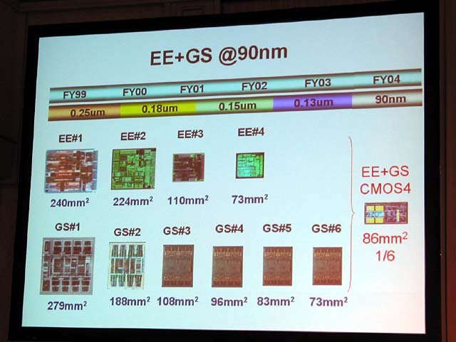
and look this picture
sony1_03.jpg

There would be some downsizing by pure logic optimization and new material, but especially in these later generations after logic optimizations on the same functions, the actual chip size shows that there was an advance in process technology between 130nm and 90nm more than anything.
 
Status
Not open for further replies.
Back
Top