You are using an out of date browser. It may not display this or other websites correctly.
You should upgrade or use an alternative browser.
You should upgrade or use an alternative browser.
TSMC wafer pricing
- Thread starter Silenti
- Start date
bigger is always better
It does feel a bit like 16nm vs 20nm… In many ways, A16 feels like N2P+backside and not much else, just like 16nm was mostly just FinFET. It’s quite disappointing N2P lost backside power delivery, that must be a very welcome surprise for Intel. I wonder how A16 compares to the *original* N2P with backside power delivery…
The density scaling is sufficiently bad that it seems to vindicate Intel’s High-NA strategy to some extent as necessary for density, although TSMC’s argument will be that doesn’t necessarily make the transistors/$ any better or significantly improve perf/power.
Still, I expect TSMC to be extremely competitive with Intel in practice for N2(non-P) vs 18A and beyond that, process nodes aren’t just about high level features and buzzwords, and TSMC has consistently delivered where it matters.
A16 is almost certainly just N2+ BSPD. I don't think it is disappointing as such given that the timing of A16 and N2P are similar. It seems to be a divergence in cost models for different applications. From TSMC's press release - "A16 ideal for HPC products with complex signal routes and dense power delivery networks", and given TSMC has chosen the most complex application of BSPD, it would certainly be a significant increase in wafer cost. TSMC has a diverse base of customers and has to cater to all possible applications/products. For those who do not need the absolute benefits of A16, N2P would be a cheaper alternative (and IP compatible with N2). Whereas for HPC, A16's benefits would probably outweigh the additional costs. Given the low number of external customers, Intel would mostly have their own internal CPU/GPU tiles on 18A, which would benefit from BSPD and hence makes sense to have on 18A. Even then I believe it is optional and can be dropped if not required.
TSMC is exploring high NA for A14 or whatever their next node is (which I expect to go to HVM in 2H'27) but they have a much higher volume than Intel and would need a significantly higher number of HNA machines. ASML would need to have the capacity to supply. Perhaps we could see them play it safe and go for High NA for A14P instead.
May 6, 2024

 wccftech.com

TSMC's Entire CoWoS Supply Reportedly Reserved By NVIDIA & AMD Until 2025
AMD & NVIDIA have reportedly reserved TSMC's entire CoWoS production for the next two years as both firms aggressively compete in the AI race.
Taiwan Economic Daily reports that TSMC has seen its packaging supply wholly booked by AMD and NVIDIA. The CoWoS technology is being used for the development of NVIDIA's Hopper and the latest Blackwell GPUs while AMD is also leveraging it for its own MI300 accelerators.
The Taiwanese semiconductor giant plans to massively scale its production facilities in response to such huge demand. The company looks to achieve around 45,000 to 55,000 units of output by the end of this year, marking a vast YoY increase. This not only shows how big of a demand the industry is witnessing but also that TSMC has shown resilience and has gone to all extents to satisfy clientele demand.
I was wondering the same and was flipping back and forth between wafers and lots.What’s a single unit of CoWoS? One wafer’s worth of stacks?
They don't specify a time period though, so...
I would have to assume it is per month and a unit is a wafer.
Edit- I was initially thinking lots because I misread the article and thought they were talking about ~50k units per year.
Edit- I guess it helps if you go to the source and ignore the shoddy journalism.
In response to huge customer demand, TSMC is actively expanding its advanced packaging production capacity. Industry estimates indicate that TSMC's CoWoS monthly production capacity will reach 45,000 to 50,000 pieces by the end of this year, a multiple increase from 15,000 pieces in 2023. By the end of 2025, CoWoS's monthly CoWoS production capacity will reach a new peak of 50,000 pieces.

台積電先進封裝產能被訂光 輝達、超微一路包到明年 | 產業熱點 | 產業 | 經濟日報
AI應用百花齊放,兩大AI巨頭輝達(NVIDIA)、超微(AMD)全力衝刺高效能運算(HPC)市場,傳出包下台積電今、明...
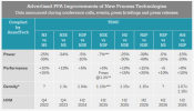
Literally from the article:Man, we're really going to go from N5(2020) to N3E to N2P to A16(2026) with a total of about 1.65x density improvement, and that only really being for logic.
Crazy times.
*Chip density published by TSMC reflects 'mixed' chip density consisting of 50% logic, 30% SRAM, and 20% analog.
Well ok, fair enough if that's the case. It just makes the numbers beyond meaningless.Literally from the article:
*Chip density published by TSMC reflects 'mixed' chip density consisting of 50% logic, 30% SRAM, and 20% analog.
Doesn't it explain why the marketing numbers are low and getting lower?Well ok, fair enough if that's the case. It just makes the numbers beyond meaningless.
They are giving a more realworld estimate of density scaling of a "typical" design.
To my knowledge, analog stopped scaling about two decades ago and SRAM has effectively stopped scaling below 5nm.
Not really. 50% of logic is a sizeable chunk in a formula and yet we're still looking at ".1x" density improvements. N5 to N3 is the last transition where there are noticeable improvements, and even that will be dissolved a bit because the difference between the most dense N5 version and the most dense N3 version will probably be smaller than between N5 and N3E from the spreadsheet.Doesn't it explain why the marketing numbers are low and getting lower?
Scaling is dead. There are no more "free transistors".
But you are comparing that to previous numbers that didn't use this more "real world" formula.Not really. 50% of logic is a sizeable chunk in a formula and yet we're still looking at ".1x" density improvements. N5 to N3 is the last transition where there are noticeable improvements, and even that will be dissolved a bit because the difference between the most dense N5 version and the most dense N3 version will probably be smaller than between N5 and N3E from the spreadsheet.
Scaling is dead. There are no more "free transistors".
TSMC listed N3 vs N5 at 1.7x but according to their "new" numbers N3E vs N5 is only 1.3x
N2's 1.15x = 1.3x
A16's 1.07x-1.1x = 1.14x-1.2x
So that would end up being >1.5x according to their old method.
Edit- They are in their incremental improvement phase since they need something new to offer every ~12-18months like they promised.
Last edited:
The "old formula" actually featured SRAM shrinkage though. Like 10 to 7nm was 0.83x fin pitch and 0.82x gate pitch for 47% higher logic density, while also HD SRAM cell size shrunk from 0.042 um^2 to 0.027. So a mix of 1.47x logic and 1.55x SRAM is in fact still 1.5x density across the chip. The issue with N3 is you're getting that same 1.5x logic, but only 1.05x SRAM, so balanced across the chip it's only 1.3x.But you are comparing that to previous numbers that didn't use this more "real world" formula.
TSMC listed N3 vs N5 at 1.7x but according to their "new" numbers N3E vs N5 is only 1.3x
N2's 1.15x = 1.3x
A16's 1.07x-1.1x = 1.14x-1.2x
So that would end up being >1.5x according to their old method.
Edit- They are in their incremental improvement phase since they need something new to offer every ~12-18months like they promised.
Though on the note of pitches, much of the density gains with 3nm are from DTCO-centric changes to standard cell layout, rather than reducing pitches. Which is also why SRAM isn't scaling, because it doesn't have extra fins to cut out.
I don't think it did... most of the time TSMC was using logic density improvements in their marketing numbers.The "old formula" actually featured SRAM shrinkage though. Like 10 to 7nm was 0.83x fin pitch and 0.82x gate pitch for 47% higher logic density, while also HD SRAM cell size shrunk from 0.042 um^2 to 0.027. So a mix of 1.47x logic and 1.55x SRAM is in fact still 1.5x density across the chip. The issue with N3 is you're getting that same 1.5x logic, but only 1.05x SRAM, so balanced across the chip it's only 1.3x.
Though on the note of pitches, much of the density gains with 3nm are from DTCO-centric changes to standard cell layout, rather than reducing pitches. Which is also why SRAM isn't scaling, because it doesn't have extra fins to cut out.
That's how N3 vs N5 went from 1.7x to ~1.3x density.
Which is my point.
People are surprised to see the node's advertised density scaling going from the expected ~1.6x-1.8x down to 1.1x when it isn't apples to apples.
https://www.anandtech.com/show/1735...n3e-in-2024-n2-in-2026-major-changes-incoming

Last edited:
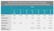
Their marketing included both logic and SRAM, separately. Whether Anandtech included SRAM cell size that in their charts is a different matter.I don't think it did... most of the time TSMC was using logic density improvements in their marketing numbers.
That's how N3 vs N5 went from 1.7x to ~1.3x density.
Which is my point.
People are surprised to see the node's advertised density scaling going from the expected ~1.6x-1.8x down to 1.1x when it isn't apples to apples.
https://www.anandtech.com/show/1735...n3e-in-2024-n2-in-2026-major-changes-incoming
View attachment 11368
But what I really meant was that up until and including N7, SRAM scaling was in line or better than logic. Advertising "logic density" or "whole chip density" as multiples would give very similar numbers, it's only N5 and below where the difference has been significant.
But I did forget that TSMC had formerly given logic and SRAM separately for N5 and N3 before switching to the whole chip metric
7nm to 5nm = 1.8x density
5nm to 3nm is only 1.3x density
3nm to 2nm is only 1.15x
2nm to 1.6nm (A16) is only 1.10x.
That is a very very worrying trend. Cache density almost reach point of non-scaling, which can be parttially ofset by stacking or chiplets. Anyway keeping Moore law alive while making new gen chips are going to be tough
Similar threads
- Replies
- 0
- Views
- 1K
- Replies
- 74
- Views
- 11K
- Replies
- 4
- Views
- 3K
- Replies
- 36
- Views
- 5K


