TSMC wafer pricing

So no die shrink for the consoles?
Eventually maybe. Sony did transition their PS5 SoC from N7 to N6 already but that's a minor change.
But so far we're seeing price *increases* on models launched in 2020 instead of price drops which would start happening on consoles 3rd year of life in the past.
 
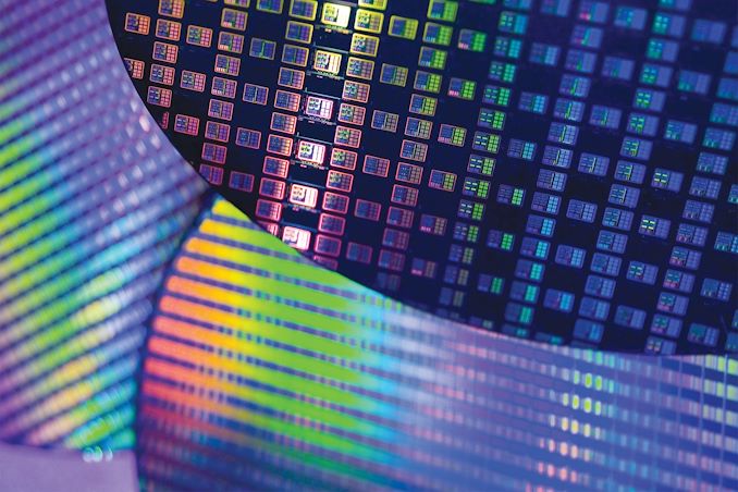
Projections indicate a notable increase in the cost of 2nm wafers compared to 3nm wafers. It is anticipated that 2nm wafers will see a 50% cost increase, reaching approximately $30,000 each. Taiwan Semiconductor Manufacturing Company (TSMC) is currently producing 3nm wafers at a cost of $20,000 per unit. The upcoming surge in prices for 2nm wafers has substantial implications for manufacturers like Apple, which faces challenges in maintaining profitability, especially for high-end products that utilize the 2nm process.
...
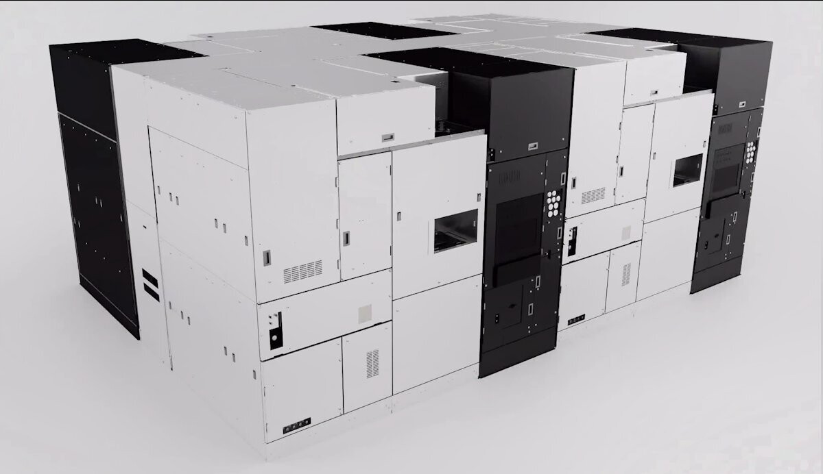
IBS estimates that a 2-nanometer fabrication facility capable of producing about 50,000 wafers monthly would cost around $28 billion, compared to $20 billion for a 3-nanometer facility. This increase is largely attributed to the need for more advanced extreme ultraviolet lithography (EUV) equipment to sustain a 2-nanometer production capacity of 50,000 wafers per month. Consequently, the production cost for each wafer and chip has risen significantly. Apple, a key user of advanced processes, is likely to be impacted by these cost changes. Presently, Apple is the sole user of TSMC's latest N3B (3nm) processors for mass production in its smartphones and PCs.
...
IBS projects that when TSMC launches its 2nm process between 2025 and 2026, the cost of each 12-inch wafer used by Apple will be around $30,000. In comparison, the cost of 3nm wafers is estimated at about $20,000. However, semiconductor news outlet Tom's Hardware has noted that IBS's chip cost estimates might be overstated. IBS approximates Apple's cost per 3-nanometer wafer at $50, but the actual cost, factoring in an 85% yield rate, is closer to $40.
...
TSMC is at a critical point as competitors, such as Samsung, are advancing in the sector. Samsung plans to start 2nm wafer production, with current pricing not yet competitive but likely to change in the future. The rapid development of artificial intelligence (AI) technology is influencing companies like NVIDIA and AMD to consider 3nm wafers and more sophisticated fabrication processes for their future products.

These advanced processes will facilitate the creation of more powerful, albeit more expensive, AI chips. NVIDIA, currently manufacturing AI chips at 5nm, already faces significant production costs. In conclusion, the differential pricing between 2nm and 3nm wafers is set to reshape the semiconductor industry, compelling companies to strategize carefully in terms of cost management and alignment with the evolving demands of technologies like AI.
 
I think this will just push the industry further in the direction of using chiplets for everything including mobile SoCs. As long as logic density keeps scaling and power keeps decreasing, which they are AFAIK, then it's not as big a deal as it sounds if you can push all of the I/O and much of the SRAM (e.g. last level cache) to a 4nm or 6nm chiplet. I suspect the generational improvement might be as good or better than 7->5nm if you did that.

Think about something like the AMD MI300X: you'd move the XCDs from 4nm to 2nm, but keep the IODs on 6nm (or maybe move IODs to 4nm especially if you want to optimise for Perf/W more than Perf/$, but there'd be no point ever moving the IODs from 4nm to 3nm really, which also has interesting implications for long-term amortisation of the production lines for different processes I suppose).
 
1.15X N3->N2 doesn't exactly scream "logic scaling" to me...
If we're referring to the same thing for 1.15X, that's for 50% logic/30% RAM/20% IO, and the assumption is that RAM/IO basically don't scale to 2nm, so achieving 1.15x would require >1.3x logic density (or even >1.35x if we assume absolutely zero scaling for IO/RAM).

Back when TSMC was quoting >1.1x rather than >1.15x about 1.5 years ago, they said >1.2x logic density iirc, so that matches it increasing to >1.3x along with the claimed 1.1x->1.15x density improvement (assuming RAM/IO still doesn't noticeably improve). I think N2->N2P is likely to give a better logic density improvement than N3E->N3P (~4%) or N5->N4 (~6%) given backside power delivery as well.

I'll admit 1.3x logic density really isn't great though, my post above was assuming more like ~1.5x off the top of my head, so it's not as bad as you might think (assuming IO/RAM can be offloaded using chiplets) but you do have a point...
 
Ooof... that sounds like it already takes into account the newer litho tools that supposedly increased throughput 30-40%.
I thought ASML was supposed to ship multiple units before the end of the year, but I've only seen the announcement from the first one going to Intel.
I have no idea on how ASML is ramping High-NA but I would assume they aren't doing more than 20-40 in 2024.
EUV-DP here we come!
High NA reduces rectile by half. So only for chipset GPUs
 
Ooof... that sounds like it already takes into account the newer litho tools that supposedly increased throughput 30-40%.
I thought ASML was supposed to ship multiple units before the end of the year, but I've only seen the announcement from the first one going to Intel.
I have no idea on how ASML is ramping High-NA but I would assume they aren't doing more than 20-40 in 2024.
EUV-DP here we come!
Not sure I understood you correctly, but TSMC is definitely not using High-NA for N2, and Intel isn’t using it for 18A anymore either.

I personally think it’s likely both Intel and TSMC will use High-NA for minor refreshes of N2/18A, similarly to how TSMC introduced EUV in N7+ and N6 which resulted in *lower* cost than DUV-only N7. Not sure if that’s N2P in TSMC’s case, it would be surprising if they introduced High-NA and backside power at the same time, but not strictly impossible.

So no, I don’t think those estimates include the (long-term at least) cost benefits of High-NA yet.

Don’t think reticle limit is really an issue at all, both because chiplets are becoming the norm and because wafer costs going up >50% means you can still build a chip ~75% as expensive as the largest chip you can make today.

I was going off the quoted article that implied the fab cost increases were due to the requirement for "more advanced EUV machines" which, in my head, meant High-NA.
Guess I might have jumped the gun there... hard to keep all the different timelines straight.

Makes sense that they both might use High-NA for their more refined processes, especially for N2P seems the most likely candidate for TSMC's longterm mainstream node.
 
Last edited:
I think this will just push the industry further in the direction of using chiplets for everything including mobile SoCs. As long as logic density keeps scaling and power keeps decreasing, which they are AFAIK, then it's not as big a deal as it sounds if you can push all of the I/O and much of the SRAM (e.g. last level cache) to a 4nm or 6nm chiplet. I suspect the generational improvement might be as good or better than 7->5nm if you did that.

Think about something like the AMD MI300X: you'd move the XCDs from 4nm to 2nm, but keep the IODs on 6nm (or maybe move IODs to 4nm especially if you want to optimise for Perf/W more than Perf/$, but there'd be no point ever moving the IODs from 4nm to 3nm really, which also has interesting implications for long-term amortisation of the production lines for different processes I suppose).
We're still talking increasing amounts of silicon for products on top of additional costs for main compute dies. 7/6nm is more affordable, but it's not reduced to some old 'legacy node' level pricing by any means. And if you want to increase amount of cache, you're gonna need to go bigger or start stacking cache on cache. All more silicon in the end.

Lack of better density scaling is definitely gonna rear its ugly head in ways going forward, even if we are technically finding ways around it in terms of pushing performance.
 
Isn't it just because it has limited supply?
More limited now than it was a quarter ago?

Apple and in some part NVIDIA have pretty much gobbled up whatever supply there was.
Nvidia doesn't seem to be making anything on the currently available N3(B).
Apple seem to be their only customer for the node right now.
The fact that it's loosing steam also likely means that nothing which is launching soon will use it either.
 
5nm also had a similar drop in revenue in Q1 2021, though not as drastic since the market conditions held.
3nm is in a pretty similar spot to 5nm, with the exception of strong market headwinds that 5nm came into, which you can see throughout 2021 to now.
 
Back
Top