Predict: The Next Generation Console Tech

Status
Not open for further replies.
28nm is theoretically 50% smaller than 40nm yet Jaguar cores will, again, have a bit of enhancements and likely require more local memory so it is not likely to fit 4 cores into the same area as Bobcat cores, even with the die shrink.

If they have a fast memory architecture such as stacked DDR4 they wouldn't need as much cache as the memory would be physically closer and higher throughput which would mean they wouldn't need as much cache, right?

But even being generous and saying 2 Bobcat cores + cache, memory controller were half a die at 75mm^2 (so about 38mm^2 for 2 cores) it would seem 2 Jaguars could (conjecture) fit into that die area on 28nm and 4 Jaguar cores into 75mm^2. 150mm^2 would be a rough guestimate to the total area needed for 8 Jaguar cores.

Considering that there are parts of the die which aren't duplicated when you raise the core count, memory controllers/uncore etc perhaps the total die area would be less than that but with so much dense logic on the chip it could jive with rumours of poor yield for the same reason that the Cell came with one disabled SPE, logic is defect intolerant. Perhaps this is the reason for the rumoured 'Xbox TV' where the lesser SKU uses the parts which don't meet spec?
 
But even being generous and saying 2 Bobcat cores + cache, memory controller were half a die at 75mm^2 (so about 38mm^2 for 2 cores) it would seem 2 Jaguars could (conjecture) fit into that die area on 28nm and 4 Jaguar cores into 75mm^2. 150mm^2 would be a rough guestimate to the total area needed for 8 Jaguar cores.

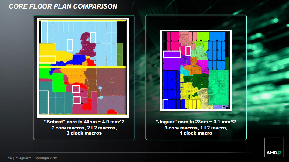
8 Jaguar cores including 4 MB of L2 cache will be smaller than 50 mm² on 28 nm, at least if you go by AMD's numbers. A Jaguar core is 3.1 mm², L2 cache is around 2 Mbit/mm² (it's probably denser than that), which gets you 24.8 mm² for the cores and 16 mm² for cache for a total of 40.8 mm². Let's just say 50 mm² to be on the safe side in other words.
 
But even being generous and saying 2 Bobcat cores + cache, memory controller were half a die at 75mm^2 (so about 38mm^2 for 2 cores) it would seem 2 Jaguars could (conjecture) fit into that die area on 28nm and 4 Jaguar cores into 75mm^2. 150mm^2 would be a rough guestimate to the total area needed for 8 Jaguar cores.

IMG0038025_1.jpg


Jaguar would be 10% larger than bobcat per core, but thanks to 28nm, it's actually smaller. Your guess figures are way off to the point of being twice as large. An 8 Core Jaguar with no GPU would likely be at most 75mm^2. In Less CPU budget than last gen they could fit 16 cores in. Actual PC jaguar products will likely have 192GCN cores for the X4 and possibly 128 for E series, maybe less for the Z series tablet APU's.

On the other hand, they won't likely be using Pitcairn, so the 8800-like chip they use will take up that extra die size saved with Jaguar. It's still less overall die size than last gen.

Let's say 75mm^2 8 core Jaguar @ 2GHz + 250mm^2 customised 8850 level GPU in an APU for a 325mm^2 chip. Reasonable, IMO. Maybe eDRAM or stacked memory on top of this for something similar or a bit bigger all up than last gen.

There was a lot of rumors of Cape Verde for Durango at one time, so dont count it out either. Pitcairn would still be very fortunate to happen imo.
 
There was a lot of rumors of Cape Verde for Durango at one time, so dont count it out either. Pitcairn would still be very fortunate to happen imo.

I'm still crossing my fingers for something with 10 times the flops of the X-Box 360, which would be Pitcairn. To be more precise, that would be Pitcairn at 940 MHz. They could go for more CUs and lower clocks to reduce TDP of course, as long as it ends up somewhere around 2400 GFLOPS. Another thing is that I hope for something Sea Island based, which is actually not too unrealistic IMO.
 
I'm still crossing my fingers for something with 10 times the flops of the X-Box 360, which would be Pitcairn. To be more precise, that would be Pitcairn at 940 MHz. They could go for more CUs and lower clocks to reduce TDP of course, as long as it ends up somewhere around 2400 GFLOPS. Another thing is that I hope for something Sea Island based, which is actually not too unrealistic IMO.

I agree, a custom 8850 at 800-900MHz should fit nicely. They could either keep the redundant CU's (from 8870) for the first revision for yield reasons or cut them off making a chip around 230-260mm^2 depending on final size of the 8870/50 and what they may add or remove from it.
 
yeah yeah definitely only on paper, many reasons.


succces of durango/orbis an all this "next gen" will be very important for AAA oriented developers. Moreso than graphical parity (not "framebuffer parity") of pc version( Pc marketd drifted away from AAA in comparison to last transition ...).I bet we will see many situations like just cause, GRAW, bad company etc when pc version was lacking significant feauters/was late outrageous port. Basicly, in many cases i expect soft touched last gen versions for pc, not for technology sake, but marketing/small target base on pc side;)Exlusives will be out of reach for budget reasons no matter how many fans we screw in pc case.
And i feel there might more of them, sonys and ms studios are growing quickly... and in this day and age will be main selling points

In addition to that, last transition devs had to learn how to deal with all these mulicore/mulithreded paradigm and even shaders in case od sony developers. This time it will be easier to bring out the performance quickly.


So yes there will be cards with paper spec much higher, especially when maxwell arrives year after... Just like last time , in many cases underperforming(x1000/7800 in graw/jc, few performing better(if game is pc port need for speed etc.)Soon after that we'll hear about new API needed (of course on another round of cards), which should bring "revolution" in pc side , but in practice will be used to make up for inefficiencies and allow second and third generation of durango/orbis games to come to pc and that 2014 cards will fade out.


This vision is somehow grim for tiny bit of pc graphics enthusiast left in me. Sadly, considering all of this, and remembering how this gen unfolded (eg. after seven years we don't have anything remotely on a scale of FEAR on pc which came out 4 years after last consoles), IQ gap will shrink again, an multi platforms are mostly uprezzed console ports.

For me this is like being happy, that in 2006 i can play quake 3 in my native monitor resolution....

If these situation is going to repeat i'll gladly see those fancy new cards only in b3d discussions.

There is so much tosh in that post that the entire post should be deleted....
 
All the AMD talk made me want to make some silicon budget comparisons.

I think there's a lot of room for improvement and customization for a console GPU. While GCN seems like a great architecture, NVIDIA is getting similar (if not better) performance with smaller chips (7970 350mm vs 680 294mm). I believe AMD can squeeze out more die size and improve efficiency, even a 15-20% savings is great and worthy of pursuit for a console.

We've been talking about CU's, what about the other units? TMU's and ROP's?

Given that resolutions are going to be limited between 720p to 1080p, can those units be trimmed down?

Pitcrain has 1280 ALU's, 80 TMU's and 32 ROP's.

I wonder if there is any kind of fixed functional blocks that they can get to provide better levels of AA. Allegedly the 360 could get free 4x AA, perhaps they can take that to the next level and get "free" (low performance hit) IQ improvements.

7970 is bigger than 680 because it has more double-precision power and so more logic to get it packed in. Pitcairn is comparable to 680 in which has DP ditched in great way to be smaller and less power hungry. You will see a 8870 similar in performance to 7970 and smaller than 680 only by going the same route as Pitcairn, ditching DP logic ( in consoles they will ditch it all ) and maybe increasing the number of TMUs. GCN is a more efficient architecture than Kepler. In fact IMHO is the best architecture from ATI ever since R300.
 
7970 is bigger than 680 because it has more double-precision power and so more logic to get it packed in. Pitcairn is comparable to 680 in which has DP ditched in great way to be smaller and less power hungry. You will see a 8870 similar in performance to 7970 and smaller than 680 only by going the same route as Pitcairn, ditching DP logic ( in consoles they will ditch it all ) and maybe increasing the number of TMUs. GCN is a more efficient architecture than Kepler. In fact IMHO is the best architecture from ATI ever since R300.

Why does everyone talk like they know for a fact what the 8870 and 8850 will be like? AFAIK we've only had unconfirmed rumors about Sea Island.
 
Why does everyone talk like they know for a fact what the 8870 and 8850 will be like? AFAIK we've only had unconfirmed rumors about Sea Island.

Because the easier way -and logical- to improve Tahiti in the same 28nm process is Pitcairn-ing that chip. It´s so good. It´s the same that made nvidia with Kepler only that accentuated by the process node reduction. 680 is a more efficient 580, achieved above all ditching thread dispatcher and DP logic...
 
It was only 'free' from a bandwidth point of view and in every other way it was no where near being 'free'

The ROPs were designed to handle 4 samples per clock just as current PC GPU parts are, so the only reason it wasn't free was in terms of shaders and the tiling requirements (obviously).

I wonder if there is any kind of fixed functional blocks that they can get to provide better levels of AA. Allegedly the 360 could get free 4x AA, perhaps they can take that to the next level and get "free" (low performance hit) IQ improvements.

Well, they ought to take a page out of nVidia's book and up the z-sampling rate. For z-only passes, Xenos was at 2Z/clk/ROP, rv770+ are at 4Z/clk/ROP, and Fermi+ are at 8Z/clk/ROP (multiply for MSAA case, of course).*


*1 ROP = 1 colour pixel out. I know the terminology changed when AMD/nVidia grouped units together
rv770 RBE = 4pix/clk, 16Z-only/clk -> 4 RBEs = 16pix/clk, 64Z-only/clk
Fermi ROP = 8pix/clk, 64Z-only/clk -> 6 ROPs -> (could only handle 8 fragments per GPC/clk, so 32pix/clk), but Z-only was the full 384/clk

As for handling proper MSAA (properly shaded/post-resolve), well, you're at the mercy of algorithms & shader power. IIRC, texture units reading back the multisamples I believe was added in Cypress so that already helps.

-----

Given that resolutions are going to be limited between 720p to 1080p, can those units be trimmed down?

Pitcrain has 1280 ALU's, 80 TMU's and 32 ROP's.
The more the better really.... ;) Shaders are going to need ALUs, TMUs for various texture sampling/filtering. Overdraw & MSAA are going to need colour & Z. Rates go down for MRTs so...

Geometry is going to need setup units.
 
We've been talking about CU's, what about the other units? TMU's and ROP's?

Given that resolutions are going to be limited between 720p to 1080p, can those units be trimmed down?
TMU's and ROP's are not really a lot more resolution dependent than are shader units. Ok for the ROP's you've got things like AA resolve passes (which doesn't need shader units), and the shader load also includes the vertex pipeline, but otherwise this is more a question about how complex your shaders are - complex shaders need more math and hence comparatively you don't need that many ROPs (and TMUs).
Besides, you cannot change the number of TMUs easily as they are tied to CUs. It would depend on the level of customization but such a gpu would really not be a HD7xxx/HD8xxx derivative (at least not a close one).
ROPs could be more easily cut down, but since everybody is expecting edram this really would make no sense - ROPs require bandwidth and are in desktop cards quite often bandwidth starved, so if you now got all the bandwidth you need thanks to edram you don't want to skimp on them imho.
 
Last edited by a moderator:
it is rumored that the jan devkit of ps4 will be close to final spec - so they have atleast to include either piledriver or steamroller cores in that apu . piledriver seems much more likly than steamroller in this time .
 
Honestly, I really dont care much about what CPU they are going to put in the next Xbox or the PS4. I think Wii U has shown the layout of what kind of architecture we would be seeing in the next generation of consoles.
 
Just out of curiosity, from where are you getting the density figure?

That's my guess based on other other processes. I think that number is actually fairly conservative, but I've not seen any proper figures from TSMC or GlobalFoundries for their 28 nm nodes.

Here is an interesting article regarding most of the current process nodes used today: http://www.realworldtech.com/iedm-2010/
An interesting quote:
real world technologies said:

According to that same article, TSMC's 28 nm node has SRAM cell sizes of 0.130 µm² per cell, although that's probably for higher density SRAM than will be used by something like Durango. IBM's eDRAM at 32 nm has a cell size of 0.0394 µm2, just remember that eDRAM cell size is smaller simply because the cells is made from different building blocks (SRAM is made from 6 or 8 transistors, eDRAM relies on a single capacitor and a single transistor). A cell size of 0.0394 µm² gives you a density of >11 Mbit/mm² according to that article. From that you could reason that a cell size of 0.130 mm² gives you a density of 3.3 Mbit/mm². I'm not completely sure if it's correct to make such assumptions though, that's why I presume a density of 2 Mbits/mm² just to be on the safe side. Intel's 4.2 Mbit/mm² is probably also a best case scenario.

Another thing you could work from is Ontario's die shot. You can find one here:http://chipdesignmag.com/lpd/pangrle/files/2012/08/barry1.png
If you simply count pixels, you can calculate that 512kB of Ontario's L2 cache is 3.2 mm² in size. Ontario is on a 40 nm node, so it's not unreasonable to say that 512 kB of L2 cache would be 1.9 mm² on 28 nm, which is assuming a scaling of just 40% (i.e. SRAM on 28 nm is just 40% smaller than SRAM on 40 nm). That would mean a density of 2.1 Mbit/mm². Much closer to my estimate, but still conservative, as I think 28 nm is closer to half the size of 40 nm, not 0.6 times the size.

Oh well, you get my drift. My opinion is that 2 Mbit/mm² is not an unreasonable estimate for SRAM density on 28 nm. It's probably even a pretty low estimate.
 
Status
Not open for further replies.
Back
Top