Predict: The Next Generation Console Tech

Status
Not open for further replies.
it is rumored that the jan devkit of ps4 will be close to final spec - so they have atleast to include either piledriver or steamroller cores in that apu . piledriver seems much more likly than steamroller in this time .

I think so too for Piledriver. But in the summer there will be the final devkit so I guess there is time for another upgrade with Kaveri (with Sea Islands GPU).

And the last cherry on top will be Volanic Islands based discrete GPU ;)
 
If you simply count pixels, you can calculate that 512kB of Ontario's L2 cache is 3.2 mm² in size. Ontario is on a 40 nm node, so it's not unreasonable to say that 512 kB of L2 cache would be 1.9 mm² on 28 nm, which is assuming a scaling of just 40% (i.e. SRAM on 28 nm is just 40% smaller than SRAM on 40 nm). That would mean a density of 2.1 Mbit/mm². Much closer to my estimate, but still conservative, as I think 28 nm is closer to half the size of 40 nm, not 0.6 times the size.

Oh well, you get my drift. My opinion is that 2 Mbit/mm² is not an unreasonable estimate for SRAM density on 28 nm. It's probably even a pretty low estimate.

Right, well if you do similar pixel counting for Trinity (each Piledriver module has shared 2MB attached), whose die size is 246mm^2 @32nm, you'll find that 2MB (16Mbit) there is ~13mm^2.

So, ~1.2-1.3Mbit/mm^2 @32nm GF.

---

And yes, Intel is not a good comparison at all. ;)

---

Mind you, we don't know who has/have won the contracts to make MS/Sony chips.
 
Right, well if you do similar pixel counting for Trinity (each Piledriver module has shared 2MB attached), whose die size is 246mm^2 @32nm, you'll find that 2MB (16Mbit) there is ~13mm^2.

So, ~1.2-1.3Mbit/mm^2 @32nm GF.
But Piledrivers L2 is also significantly faster (runs at up to about 4 GHz while Bobcat's and Jaguar's half speed L2 is running at 0.8 to maybe 1.2 GHz tops; the absolute latency of Bobcat's L2 is about twice that of Piledriver's L2 despite the smaller size and the simpler function [dedicated vs. shared cache]) and uses a completely different SOI process with a nominally larger feature size. That's very hard to compare.

The numbers we have is that the 0.5 MB of L2 in TSMC's 40nm we see with Bobcat are measuring about 3.0 mm² (~1.3 MBit/mm²). And SRAM and cache arrays tends to scale very well (also with more restricted layout rules as the structures are extremely regular). It is reasonable to assume about 2.5 Mbit/mm² on TSMC's 28nm for an L2 cache with the speed and latency requirements as seen for Bobcat and Jaguar (but Jaguar adds some overhead in the cache controller for the handling of the sharing between the cores, but saves something because there is only a single cache controller and not multiple copies for each core). That means a 2 MB Bobcat style L2 cache in TSMC's 28nm would probably measure just 6.5 mm² or so. Even being generous with the die space needed for the shared cache control, it will hardly push it well over 10mm².

Or see it the other way around. Bobcat measured 4.6mm², the 512kB cache ~3.0 mm², i.e., the cores were significantly larger than the cache. According to AMD, Jaguar adds about 10% or a bit more size to Bobcat on the same process. But the L2 per core stays the same. That means the relative die size of the cache should be shrinking, especially as caches often scale better than logic. But just assuming the same ratio of core area to cache area, we would end up with about 20.5 mm² . That would actually allow for a similar increase of the relative cache area (for the more complicate control logic) as seen for the cores. So less than 25mm² for a quad core Jaguar CU on TSMC's 28nm is really a quite safe bet. 25mm² would actually require 12 mm² for the 2 MB L2 cache. That is what 4 copies of Bobcat's L2 in 40nm measure. The bet can't get much safer. There is some wiggle room if MS chooses to fab the chips at GF. But GF actually claims a superior density with their 28nm bulk process compared to TSMC's 28nm.
 
Last edited by a moderator:

Fair enough. :)

How much of an effect is there with cache associativity? Jaguar's is supposed to be 16-way vs Bobcat's 4-way, for instance.
uses a completely different SOI process with a nominally larger feature size. That's very hard to compare.
Indeed. ;) We have heard of MS double/triple sourcing for Oban, and Jaguar is supposed to be more easily portable between foundries, so...
 
How much of an effect is there with cache associativity? Jaguar's is supposed to be 16-way vs Bobcat's 4-way, for instance.
I would guess it was relatively cheap to quadruple the associativity. The actual L2 cache (consisting of 4 banks with 512kB) is basically unaffected by this. The increased work is done when checking the central tags in the shared cache controller (which [together with the tags] supposedly runs at core speed, not at half speed as the the cache itself). As I said, the cache controller is some area where Jaguar differs from Bobcat. Compared to a hypothetical quad core Bobcat, there is now only a single controller which does a bit more instead of four individual controllers (+ some part of the northbridge providing the glue). AMD actually said that the shared controller enabled some synergies (saved transistors) compared to several copies of individual ones probably balancing the increased capabilities at least partially.
Or to make it clearer with a simplified example: An access of an 4way associative cache requires the check of 4 tag entries (usually done in parallel, so there are 4 logic blocks for the checks working in parallel). Having four 4way associative caches means there are 16 such blocks, the same as for a single 16way associative cache.
 
Last edited by a moderator:
Honestly, I really dont care much about what CPU they are going to put in the next Xbox or the PS4. I think Wii U has shown the layout of what kind of architecture we would be seeing in the next generation of consoles.

Yeah. If they manage to implement full HSA, sharing of work between CPU and GPU will become much more efficient, rendering even very small CPU cores viable.

In this stage of speculation, I'm much more interested in total TDP, ram configuration, bandwiths, and info about existence of dedicated GPUs.
 
Finally I can put my old SCSI drives to use again. Reliable, dependable, fast and more shock proof: perfect for Xbox tablet gaming on the go.
 
I think so too for Piledriver. But in the summer there will be the final devkit so I guess there is time for another upgrade with Kaveri (with Sea Islands GPU).

And the last cherry on top will be Volanic Islands based discrete GPU ;)
Lets not get too ambitious. :) Volcanic Islands [9xxx] is targeted to be 20nm part, and I simply cant see mass production of highpowered 20nm chips in late 2013. I want new consoles in 2013 damnit! :D
I would wait for Volcanic Islands with zero regrets.
 
Yeah. If they manage to implement full HSA, sharing of work between CPU and GPU will become much more efficient, rendering even very small CPU cores viable.

In this stage of speculation, I'm much more interested in total TDP, ram configuration, bandwiths, and info about existence of dedicated GPUs.

I would still want a proper CPU though. You can't offload everything to your GPU, making a decent performing CPU crucial. To me Jaguar at 1.6 or maybe even 2 GHz would be good enough though, and then as many cores as they think reasonable.
 
Lets not get too ambitious. :) Volcanic Islands [9xxx] is targeted to be 20nm part, and I simply cant see mass production of highpowered 20nm chips in late 2013. I want new consoles in 2013 damnit! :D

Wouldn't hold my breath on it either but I think there's a chance we could see it happening if Sony decide to wait for it and launch in 2014. Afterall there's still the puzzle of the 'Milos' codename which we haven't figured out yet :)

Volcanic Islands said:
Manufactured at 20nm Gate-Last process, this will be the first GPU family which AMD should be able to manufacture in Common Platform Alliance as well as its long-standing foundry partner, TSMC. Thus, AMD will have the choice between TSMC GigaFab Hsinchu/Taichung, IBM East Fishkill, GlobalFoundries in New York and Dresden or Samsung in Austin. The manufacturing flexibility will be of paramount importance, for Volcanic Islands GPU architecture will represent the pinnacle of system integration between the CPU and GPU

Bodes well for future production of the chips on that process if true.
 
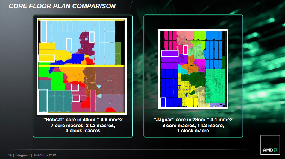
8 Jaguar cores including 4 MB of L2 cache will be smaller than 50 mm² on 28 nm, at least if you go by AMD's numbers. A Jaguar core is 3.1 mm², L2 cache is around 2 Mbit/mm² (it's probably denser than that), which gets you 24.8 mm² for the cores and 16 mm² for cache for a total of 40.8 mm². Let's just say 50 mm² to be on the safe side in other words.

IMG0038025_1.jpg


Jaguar would be 10% larger than bobcat per core, but thanks to 28nm, it's actually smaller. Your guess figures are way off to the point of being twice as large. An 8 Core Jaguar with no GPU would likely be at most 75mm^2. In Less CPU budget than last gen they could fit 16 cores in. Actual PC jaguar products will likely have 192GCN cores for the X4 and possibly 128 for E series, maybe less for the Z series tablet APU's.

On the other hand, they won't likely be using Pitcairn, so the 8800-like chip they use will take up that extra die size saved with Jaguar. It's still less overall die size than last gen.

Let's say 75mm^2 8 core Jaguar @ 2GHz + 250mm^2 customised 8850 level GPU in an APU for a 325mm^2 chip. Reasonable, IMO. Maybe eDRAM or stacked memory on top of this for something similar or a bit bigger all up than last gen.

I know I was over-estimating. But I don't think taking Jaguar being 10% bigger at the core-level on the same process is the end of the story. 4, or 8, cores is going to require more memory--probably per core and a probably an L3. And more cores is going to need more bandwidth so your memory bus is going to be larger and since the bus can only be so small that could factor into overall size.

My post was actually two fold in subtle points: #1 was to look at the AMD APU rumors and could they work. One way to look at that is the size and power. 4, even 8, Jaguar cores and a Pitcairn class GPU fall *under* the footprints of last gen consoles. Going out of the gate with a SoC with such a large GPU (has this ever been done??) would be a challenge but for the size issue it looks possible. And it could well align with the idea of stacked memory on an SI in one neat, elegant package. So the rumor is at least possible--more possible than the x86, PPC, and ARM processors all in ONE console.

The #2 point was tongue in cheek... such hardware would be a big step back in terms of silicon investment. I know it is chick and popular to downplay the millions of hardcore gamers but as elegant as the above solution is (neat imo) I would hope for something more beefy. Anything less would be very disappointing in my opinion because something of this nature is surely possible.

But because of that it makes it seem even more likely to me ;) I could easily see Sony roll out a 4 core + Pitcairn class GPU on an SI with stacked memory. In fact I think such a console would be pretty fast, possibly affordable, definitely minimize risk, etc.
 
Please, no L3 is needed - you can't do without a L3 on the Intel architecture but it's optional on its AMD counterparts, K10.5, Stars, Bulldozer v1 and 2.
Bandwith needed by the CPU isn't that big either, the A10's CPU is roughly as powerful as an 8 core Jaguar but uses 128 bit ddr3 with a GPU to feed as well.
 
Not only is L3 not needed, adding it would mean a major redesign of the caches. The L2 in Jaguar is a Last-Level Cache, with the logic to handle coherency. If another cache level was added, it would go between it and the L1. To add a L3 after it would mean ripping out huge parts of the design.
 
Is it just me but are a lot people just posting links and pictures with a few words tacked on?

How is posts like that helping this discussion?

Anyway, do we have any idea/evidence of what power limit they'll be going with?

I personally can't see them going up to 300w, maybe 250w at the absolute max? PS3 originally pulled ~210w so 250w wouldn't be out of reach of possibility.
 
Status
Not open for further replies.
Back
Top