Predict: The Next Generation Console Tech

Status
Not open for further replies.
How close is the current chip to being pad limited?
No idea. But wishful thinking, if the shrink is modified to be used on a 2.5D interposer, would that solve the issue of pad area? The vias don't need much space nor much power. Not an off-the-shelf part anymore, but not nearly a complete redesign.
The clock scaling from a 45nm part to 32nm with the same design has turned out to be in the tens of percent, not more than doubling.
If a chip is going to go for 4GHz, it is going to be designed for it and would probably get close to that speed at 45nm.
Ah oups :oops: Still there a bit of wiggle room, A2 has a max of 2.3Ghz, 45nm, 65W for the 16 cores version.

How about waiting for 20nm and have twice the cores, maybe around 200mm2? Suppose IBM have planned all along to have twice the number of cores on their next A2 chip, they have a 4-cores, a 16-cores, an 18-cores, the one in development could be 32 or 36. It still doesn't have to be a custom chip, just the next one IBM has planned for their own needs, with some modification to the memory I/O and maybe put it on an interposer.
 
Probably a silly question, but is there perhaps any chance that the x86 CPU could also have SPUs embeded?

Is that even remotely possible?

Really hoping for BC:devilish:

On the other hand, if true i'd be quite impressed to see a new Sony Console going for broke again to give us a true next-gen console with a 10year life-cycle.

I'd buy that :cool:.
 
No idea. But wishful thinking, if the shrink is modified to be used on a 2.5D interposer, would that solve the issue of pad area?
If large parts of the chip are redesigned, a lot of things can be done to allow the design to shrink more smoothly.


Probably a silly question, but is there perhaps any chance that the x86 CPU could also have SPUs embeded?

Is that even remotely possible?
It's not really possible, at least not with any definition of "embedded" I can think of in this context.

Really hoping for BC:devilish:
Either they tell you to buy a PS3 Slim, or they provide a separate module or chip with PS3 chips on it.
 
Wow, kicked off the ranch already eh? That was quick! :oops:

So what's your opinion of the Sony AMD APU deal?
Breaking NDA is a pretty serious crime in the gaming world, even if it theoretically is something that was "known" or "rumored".
I have no idea about the Sony APU deal, makes sense though, since, as we've seen, Sony isn't all that concerned about backcompat.
 
Really hoping for BC:devilish:
On the other hand, if true i'd be quite impressed to see a new Sony Console going for broke again to give us a true next-gen console with a 10year life-cycle.
I'd buy that :cool:.
If they come out with an optional BC module, and still put the best hardware they can in the PS4, how much would you be ready to pay for the module? Myself I'd pay up to 100$. If there's no way to have hardware-based BC I'm not buying the PS4. The software emulation angle has been all kinds of pain every time someone tried it. They say it runs 90% of games, and all the best games that really pushed the machine are in that missing 10%. Having multiple consoles and multiple controllers is also a pain. That PS3 has to go as soon as the PS4 takes that shelf space. I wouldn't have bought the PS3 if it didn't work perfectly with my PS2 discs.

That module could be integrated in the Premium SKU and be optional for lower cost SKU. But they HAVE to give the option.
 
Charlie's article is up and it's stupid

http://semiaccurate.com/2012/03/02/sony-playstation-4-will-be-an-x86-cpu-with-an-amd-gpu/

He says Sony is pursuing 3D stacking, in order to make even more massive chips.

Never mind that:

-Is there any chance 3D stacking is commercially ready in 2013-14?
-Why bother? The top normal GPU's are likely outside the thermal limits of a console anyway. Therefore if it's raw power you're pursuing, 3D stacking is irrelevant.
-He also says its an SOC or could be an SOC at points, again if you're pursuing max power that in itself is contradictory
-Sony's financial status probably precludes them losing a ton of money on PS4, and the only other option is price it really high and that's no option after PS3 debacle.

My point is if you're looking to outmuscle the other guy you almost surely dont need exotic 3D stacking to do it. Just get a bigger GPU than him.

I think Charlie just read this article and made up the rest with his imagination. Since he seemed really a bit crazy with some of his Kepler reporting too I'm beginning to seriously doubt his credibility.


Stack simple nand gate array would consume very little energy, and would accelerate arbitrary functions in hardware Memory processor integration massive parallelism intrinsic
 
It means you can't just blindly pull numbers out of thin air. We already saw how awful the scaling was for 45nm cell.

Where do you assert that I'm blindly pulling numbers? The slim demonstrably uses less than half the power of the original PS3. I asserted that power drops by a factor of 0.7 per node drop, supported by the fact that there have been two full node drops and power is less than half. http://www.ps3devwiki.com/wiki/SKU_Models#Retail_Models

90nm to 45nm is two full node jumps (65nm); the half-nodes are 80nm, 55nm etc. Transistors scale in more than one dimension, so ideally, you would expect 50% reduction in size after each node. A 0.7 factor is actually very shitty.

Yeah, I'm talking about power scaling, not area scaling. It's about half for each full node drop, as you note. You typically reduce to 65 to 70% of original minimum dimension, square it and you get your half the area number.

The 90nm Cell SPE could run at 3.2 GHz at a little over .9V, possible a bit higher with margin.
A 28nm ARM test chip that was touted a while back operates at .85V.

Voltage is not scaling all that well, particularly at the multi-GHz range.

Thanks for that fix. I definitely exaggerated the progress made there. Makes more interested in Intel's STV efforts now.
 
Last edited by a moderator:
You said so yourself, there is no 28nm PS3.

You have me thoroughly confused. What was I saying with regards to a non-existent 28nm PS3 design that you have an issue with? I made a generalization about process shrinks as they relate to power savings and area in order to show how an 8x order of magnitude in compute power was feasible, but I don't see how you could have issue with that. You'd have to buy the idea that that much less area and power directly translates to scaling to 8x more power, which is much more far-fetched than another 0.7 reduction on power usage by going to 28nm, if you ask me.
 
I just don't think it's a good idea to make a trend with just 90nm and 45nm figures. The 65nm power figures become dubious because of the mix of processes during the transition period.

No biggie.
 
I just don't think it's a good idea to make a trend with just 90nm and 45nm figures. The 65nm power figures become dubious because of the mix of processes during the transition period.

No biggie.

I see. You can actually compare 90/90, 65/90, 65/65, 45/65 and 45/40 (CPU/GPU) numbers though in this chart http://www.ps3devwiki.com/wiki/SKU_Models#Retail_Models

It just becomes harder when you want to look up the actual power tests. Still, if you go by W rating on the supplies, you go from 200 at 90/90 to 130 at 65/65 to 80 at 45/40. 65% and 61.5% respectively, so my 70% number was a little conservative.
 
I said it earlier Power A2 are not limited to 2.3GHz. I guess I've to go through the pain of doing the research...

http://www.theregister.co.uk/2010/02/09/ibm_wire_speed_processor/

Took me / I lost 10 minutes researching that.
Sorry I missed it completely. So it's up to 3Ghz at 45nm. It's still vague, are they talking about the PowerEN chip only, or is that statement also applicable to the BluGeneQ?

3.2Ghz, 28nm, 16 A2 cores, 180mm2 = 800 Gflops SP
3.2Ghz, 20nm, 32 A2 cores, 200mm2 = 1600 Gflops SP
 
I wonder if it's similar to SPE's that were somewhere around "up to" 5GHz at 90nm :)
IBM's argument does sound similar to the 3.2Ghz Cell although it could be cloked at 4Ghz from the start, they clocked it lower for better efficiency.

I guess the question is, what's more expensive between a larger power supply for higher clocking, versus a CPU with more cores clocked lower for efficiency? There has to be a difficult balancing act there...
 
Sony never change.. Please.

The good thing is Sony/MS are setting huge pressure on each other. If one goes crazy on tech the other needs to "respond".

I can imagine Epic sending messages how UE4 will looks better on this or that..
 
Last edited by a moderator:
Power use balloons once a design is clocked near the top end of its range because it requires higher voltages. Other factors such as sensititivity to variation and teething problems with the process become more acute as well.

However, it's not always the case that having more cores is sufficient to replace one power-guzzling large core.
It's particularly true of the reasonably power-efficient SPE.
A workload that really shines with a local store and narrow high-clocked SPE may not be satisfied by the same number of FLOPs divided amongst several slower cores.
Straight-line performance can still matter, and in the case of backward compatibility, it isn't easy to automatically make code that works on a single SPE distribute itself amongst several processors.
 
If PS4 is AMD x86 + GPU, Sony will likely include Cell in there for BC, maybe a physics processor or something. Cell will be really small by then and maybe can be clocked faster too, delivering cheap FLOPS for scaling or fine tuning stuff for image quality.

If AMD managed to convince Sony to use their piledriver or newer core, maybe they might have their edge back on gaming side CPU on PC over Intel if dev managed to optimise game for their unique CPU core. So maybe AMD might cut some of the cost to Sony for PS4.

If Sony go with Intel for x86 CPU, they probably pay a very expensive price, like how MS did with Xbox.

I don't think what CPU cores they end up using matters anymore, it's all about the GPU anyway.
 
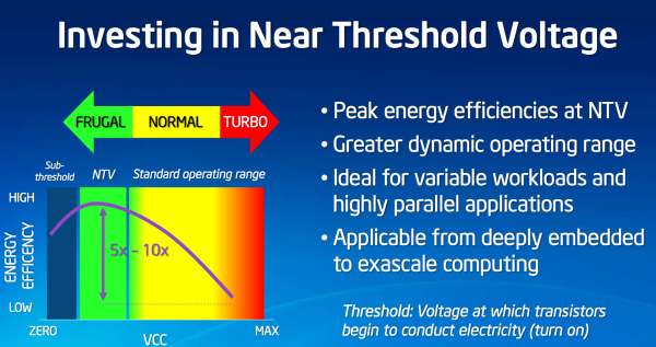
This is a good (simplified) reference for energy efficiency vs. operating voltage.

http://www.anandtech.com/show/5555/intel-at-isscc-12-more-research-into-near-threshold-voltage

Specifically
Screen%20Shot%202012-02-20%20at%2012.59.47%20PM_575px.png
 
If PS4 is AMD x86 + GPU, Sony will likely include Cell in there for BC, maybe a physics processor or something.
"In there" where exactly? For decent backwards-compability it will need around 25GB/s to RAM + similar amount to GPU, pretty much the only way to get it is to integrate it either inside or VERY close to the CPU/GPU.
 
Status
Not open for further replies.
Back
Top