I could see that INT SIMD unit could be extended with FP math for Celestial. Turing's 1:1 share for FP:INT was unbalanced.Oh yeah I forgot Nvidia is SIMD16. Battlemage looks a bit like Turing.
Install the app
How to install the app on iOS
Follow along with the video below to see how to install our site as a web app on your home screen.
Note: This feature may not be available in some browsers.
You are using an out of date browser. It may not display this or other websites correctly.
You should upgrade or use an alternative browser.
You should upgrade or use an alternative browser.
Intel ARC GPUs, Xe Architecture for dGPUs [2022-]
- Thread starter BRiT
- Start date
I think Volta/Turing's architecture has been partly misunderstood tbh, the 32x32+32 integer multiply-add was the same pipeline as the FP32 FMA reusing some of the HW, so the "integer" path was mostly just the cheap stuff like integer add, bitwise ops, etc... and a key benefit of "underpowering" the FP path is that it meant there was spare instruction fetch/decode performance not just for INT but also control ops like branches etc... which used to be effectively 'free' on Volta/Turing but now effectively prevent the 2nd FMA (or a special function op like rcp/log/etc.) from being co-issued so each control op is quite expensive. The extra FP32 FMA is cheap so it's a clear PPA win but the previous design made a lot of sense, and now it's the fetch/decode that's a bottleneck (which should be cheap area-wise, but hard to increase the throughput of architecturally given how everything else works).I could see that INT SIMD unit could be extended with FP math for Celestial. Turing's 1:1 share for FP:INT was unbalanced.
To go back to Intel GPUs, I've never seen much information at this level of detail on how their execution ports work, but based on Figure 4 of Page 5 here, it looks to me like they don't have FP/INT co-issue at all on the "Xe-LP" parts and the Port 1 for "EM" is just for special function (log/exp/rcp/rsq/etc.) but they do allow co-issue of Branch instructions (and SEND, not sure what those are, fragment/vertex output and blending?). So that *might* just be a simple dual-issue with INT/FP on one side and EM/BRANCH/SEND being co-issuable, or something more complex.
But then they have 3 ports on Xe-HPG: FP + INT/EM + XMX... I am a bit skeptical (from my own personal GPU HW architecture experience) of merging the INT & EM ports, because EM is really quite special, they are all "single source, single destination" operations and higher internal latency than most other things (although potentially similar to an INT32 multiply-add if you optimise them a certain way). Just like everything Intel GPUs, AFAICT they seem to gravitate towards more and more complexity with dubious high-level architectural choices like SIMD8/SIMD16 hurting their PPA more than all the same clever tricks put together *shrugs*
Also I wouldn't say NVIDIA is SIMD16, because their register files are physically SIMD32 (2 banks at SIMD32 means an effective 4 reads + 4 writes at SIMD16 per cycle), and you cannot get more than 50% throughput for half-filled warps under *any* cirumstance (unlike on G80, where such a mode did exist for vertex shaders, but even one of their lead compute architects I spoke with in person back in 2008 didn't know about it!) - my assumption is that Intel can achieve 100% throughput for SIMD16 on Battlemage which is a very different set of trade-offs.
This hits home hard though - I've had to argue that exact same thing at previous GPU employers repeatedly over the years sadly, too many GPU architects try to be too clever in their own unique way, and it rarely works out in practice for exactly that reason. Because AMD has both consoles, if you're "AMD-like" rather than "NVIDIA-like" then you're possibly okay as well, but doing something completely different with its own unique unexpected performance cliffs that developers might not expect and certainly won't optimise for is asking for trouble...The dominant expectation Petersen talks about is a sort-of graphics programming zeitgeist—it's whatever the done thing. As Petersen later explains, the done thing in graphics is whatever "the dominant architecture" does, i.e. Nvidia.
Also I wouldn't say NVIDIA is SIMD16, because their register files are physically SIMD32 (2 banks at SIMD32 means an effective 4 reads + 4 writes at SIMD16 per cycle), and you cannot get more than 50% throughput for half-filled warps under *any* cirumstance (unlike on G80, where such a mode did exist for vertex shaders, but even one of their lead compute architects I spoke with in person back in 2008 didn't know about it!) - my assumption is that Intel can achieve 100% throughput for SIMD16 on Battlemage which is a very different set of trade-offs.
Good point. Operand fetch and instruction issue are probably both SIMD32 issuing to each hardware SIMD16 block in alternate clocks.
I know it hurts your ego. I was in the same position. But the only rational decision is to follow the standard, unless you have something that gives a substantial performance advantage (not in a subroutine test but in overall fps) and that the majority of developers will implement (which is the hardest part when you are not the dominant player). Kudos Arun for your honestly on this topic, I feel it's kind of taboo in the engineering world, yet the reason of so many failures...This hits home hard though - I've had to argue that exact same thing at previous GPU employers repeatedly over the years sadly, too many GPU architects try to be too clever in their own unique way, and it rarely works out in practice for exactly that reason. Because AMD has both consoles, if you're "AMD-like" rather than "NVIDIA-like" then you're possibly okay as well, but doing something completely different with its own unique unexpected performance cliffs that developers might not expect and certainly won't optimise for is asking for trouble...
Game developers don't write/test their applications against some theoretical gfx API specs! They've ALWAYS developed their applications against concrete driver implementations of these said gfx APIs so what Petersen articulated shouldn't really come out as some astonishing revelation. There's going to be developers out there who'll continue to indefinitely brush aside Intel gfx HW ...
digitalwanderer
Legend
Good on them, I hope to see Xe2 supporting all new titles day 1!
D
Deleted member 2197
Guest
Stacking Up Intel Gaudi Against Nvidia GPUs For AI
Here is something we don’t see much anymore when it comes to AI systems: list prices for the accelerators and the base motherboards that glue a bunch of
 www.nextplatform.com
As Intel revealed back in June 2023, the Falcon Shores chips will take the massively parallel Ethernet fabric and matrix math units of the Gaudi line and merge it with the Xe GPU engines created for Ponte Vecchio. This way, Falcon Shores can have 64-bit floating point processing and matrix math processing at the same time. Ponte Vecchio does not have 64-bit matrix processing, just 64-bit vector processing, which was done intentionally to meet the FP64 needs of Argonne. That’s great, but it means Ponte Vecchio is not necessarily a good idea for AI workloads, which would limit its appeal. Hence the merger of the Gaudi and Xe compute units into a single Falcon Shores engine.
We don’t know much about Falcon Shores, but we do know that it will weigh in at 1,500 watts, which is 25 percent more power consumption and heat dissipation of the top-end “Blackwell” B200 GPU expected to be shipping in volume early next year, which is rated at 1,200 watts and which delivers 20 petaflops of compute at FP4 precision. With 25 percent more electricity burned, Falcon Shores better have at least 25 percent more performance than Blackwell at the same floating point precision level at roughly the same chip manufacturing process level. Better still, Intel had better be using its Intel 18A manufacturing process, expected to be in production in 2025, to make Falcon Shores and it better have even more floating point oomph than even that. And Falcon Shores 2 had better be on the even smaller Intel 14A process, which is expected in 2026.
It is past time for Intel to stop screwing around in both its foundry and chip design businesses. TSMC has a ruthless drumbeat of innovation, and Nvidia’s GPU roadmap is relentless. There is an HBM memory bump and possibly a GPU compute bump coming with “Blackwell Ultra” in 2025, and the “Rubin” GPU comes in 2026 with the “Rubin Ultra” follow-on in 2027.
Oh, wow. I can't even...
Is this an AI gone AWOL or is it my non-native language skill not being sufficient?

Is this an AI gone AWOL or is it my non-native language skill not being sufficient?

Subtlesnake
Regular
Portland, Oreogon. That must be where the Oreos get made.Oh, wow. I can't even...
Is this an AI gone AWOL or is it my non-native language skill not being sufficient?

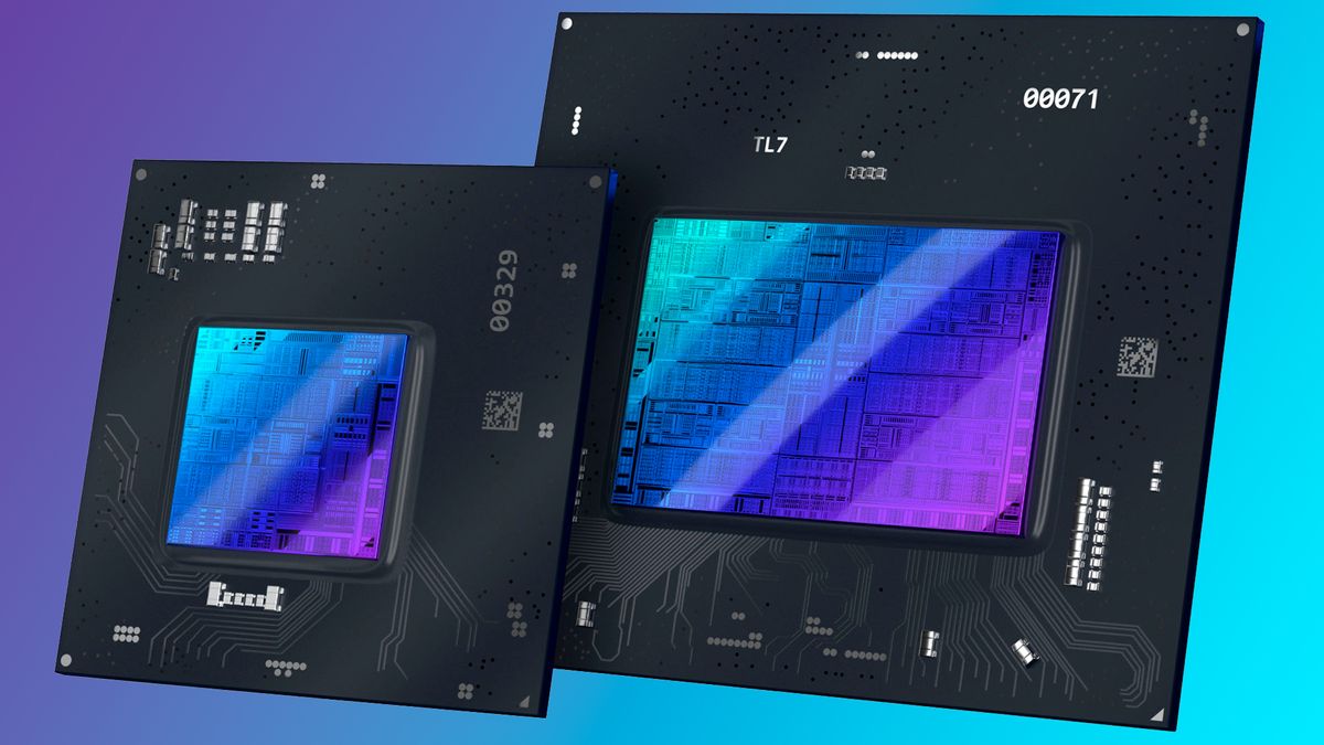
Intel prepping at least five new Battlemage GPU models — new PCI IDs added to Linux 6.11 kernel
Battlemage could debut with far fewer discrete GPU SKUs compared to Arc Alchemist
Frenetic Pony
Veteran
Alright actual info! Let's look at the leaked Lunar Lake Timespy Scores (cause that's about all we have for benchmarks so far): 4151 Lunar Lake 30w
Then we'll compare it to an RTX 4070ti: 22824 Timespy
Assuming the Timespy is the 8 "Core" Xe variant, a good guess, and the leaked 32 core dedicated GPU puts us at 16604, hopefully clockspeed goes a good deal above that for a 4070s performance
I guess it depends entirely on price, a 16gb 4070s for $499 would be decent, maybe they can push it all the way up to a 4070ti+, I'm assuming the 17w lunar lake is about 1.7ghz and max clockspeed here (> 4070ti) is about 2.5ghz.
Last edited:
Intel's performance in Timespy does not always translate to similar performance in actual games though, but it is still a step forward definitely. Both Lunar Lake and Panther Lake are shaping up to be competent products.A few asterisks but great perf and efficiency gains for Intel's iGPUs in general the last few years, competent integrated graphics for all
With the caveat mentioned above, the dGPU would also have the benefit of significantly higher memory bandwidth. Assuming 256 bit GDDR6 at 20 Gbps, it would have 5.33x the bandwidth vs 128 bit LPDDR5-7500, which would be needed esp if they get good clocks. Could be a fairly competent product for $499 or thereabouts.Alright actual info! Let's look at the leaked Lunar Lake Timespy Scores (cause that's about all we have for benchmarks so far): 4151 Lunar Lake 30w
Then we'll compare it to an RTX 4070ti: 22824 Timespy
Assuming the Timespy is the 8 "Core" Xe variant, a good guess, and the leaked 32 core dedicated GPU puts us at 16604, hopefully clockspeed goes a good deal above that for a 4070s performance
I guess it depends entirely on price, a 16gb 4070s for $499 would be decent, maybe they can push it all the way up to a 4070ti+, I'm assuming the 17w lunar lake is about 1.7ghz and max clockspeed here (> 4070ti) is about 2.5ghz.
Though it'll likely be on TSMC 5nm family process, not 3nm.With the caveat mentioned above, the dGPU would also have the benefit of significantly higher memory bandwidth. Assuming 256 bit GDDR6 at 20 Gbps, it would have 5.33x the bandwidth vs 128 bit LPDDR5-7500, which would be needed esp if they get good clocks. Could be a fairly competent product for $499 or thereabouts.
2.5Ghz is certainly doable on 5nm as well if that's the estimate being used here, though.
And I would hope for better than $500 for such a product. 4070S like performance for $500 is absolutely nothing to be excited about at all.
DegustatoR
Legend
Everyone should brace themselves for worse than expected performance due to drivers IMO. Just like Alchemist this one will do well in some benchmarks but will completely fall apart in others and the average results will be worse than you'd think. A 4070S level performance at $500 would be a bit above where the card would need to sit price wise to be competitive probably. It is also coming at the end of current generations from both competitors so any comparisons to 40/7000 series will be irrelevant rather soon.
Yes unlikely to be 3nm, not enough capacity and certainly not cheap enough yet. Likely to be N4P I suppose.Though it'll likely be on TSMC 5nm family process, not 3nm.
2.5Ghz is certainly doable on 5nm as well if that's the estimate being used here, though.
And I would hope for better than $500 for such a product. 4070S like performance for $500 is absolutely nothing to be excited about at all.
Well the 4070S 12GB still sells for ~$600 so if you get a 16GB card with similar performance for $499 it's not a terrible deal (assuming they've gotten the drivers sorted). Though N48 should be even better and rumoured to be ~$599 so Intel would be a tough sell.
True, one would hope Intel have gotten the drivers sorted by now, it's been almost 2 years now. If I remember correctly, there were a lot of issues in older titles in particular (and this is even more relevant for IGPs). And yes next gen are due from both Nvidia and AMD so the product stacks would change by the time it comes to market.Everyone should brace themselves for worse than expected performance due to drivers IMO. Just like Alchemist this one will do well in some benchmarks but will completely fall apart in others and the average results will be worse than you'd think. A 4070S level performance at $500 would be a bit above where the card would need to sit price wise to be competitive probably. It is also coming at the end of current generations from both competitors so any comparisons to 40/7000 series will be irrelevant rather soon.
It's devastatingly depressing how much consumers seem to have forgotten what a new generation of GPU's is supposed to bring in terms of performance-per-dollar improvements.Well the 4070S 12GB still sells for ~$600 so if you get a 16GB card with similar performance for $499 it's not a terrible deal
What you're talking about is an absolutely abysmal generational improvement in value. Crumbs.
I mean, good lord, we used to expect the new $400 GPU to match the last gen's highest end GPU! Even if that's not feasible anymore, there's still a huge middle ground between this and just getting a 15% discount at a given performance level after two freaking years...
Similar threads
- Replies
- 90
- Views
- 18K
- Locked
- Replies
- 1K
- Views
- 235K
- Replies
- 70
- Views
- 22K
- Sticky
- Replies
- 1K
- Views
- 396K