You are using an out of date browser. It may not display this or other websites correctly.
You should upgrade or use an alternative browser.
You should upgrade or use an alternative browser.
AMD Vega Hardware Reviews
- Thread starter ArkeoTP
- Start date
DavidGraham
Veteran
I saw this pop up a lot during our stream yesterday, that the driver isn’t meant for gaming so it hasn’t been optimized for gaming. Instead, it’s only targeting “professional” level applications. First, that’s not the case and AMD has confirmed that. The driver has all the gaming optimizations that the other Radeon drivers would include up until at least the driver branching mentioned above. After that time, optimizations may or may not have made it in, as AMD tells it.
The one caveat to this is that the Vega architecture itself is still unoptimized in the driver. But this would affect gaming and non-gaming workloads most of the time. So if the driver isn’t ready for ANYTHING, then that’s a valid concern, but it applies to ALL workloads and not just games.
https://www.pcper.com/reviews/Graph...B-Air-Cooled-Review/Answering-Questions-you-A
Die shot

Edit: The power draw doesn't look pretty:

Why does it need so much power?
Edit: The power draw doesn't look pretty:
It's going to be one of those cards again where reducing voltages actually improves performance. Depending on your luck of course.
It's going to be one of those cards again where reducing voltages actually improves performance. Depending on your luck of course.
Almost every card these days improves with undervolting. You can get 1600-1700 core clock at 160 watts with Pascal GP102 at 0.800mv, I'm guessing that what they are setting for those new laptop 1080s. I just wish that we'd get an undervolting section in reviews, it's probably more interesting than overclocking is these days
More detailed PCB overview:


From: https://www.pcper.com/news/Graphics-Cards/Radeon-Vega-Frontier-Edition-GPU-and-PCB-Exposed


From: https://www.pcper.com/news/Graphics-Cards/Radeon-Vega-Frontier-Edition-GPU-and-PCB-Exposed
- Die size: 27.85mm x 20.25mm (GPU only, not including memory stacks)
- Area: 564mm2
- Package size: 47.3mm x 47.3mm
- Area: 2,237mm2
Can that chip area be double-checked?
Fiji is 593mm2.
Kind of weird how close the area gets to Vega if it just "lost" two HBM interfaces. Where'd all the area savings from 14nm go?
Fiji is 593mm2.
Kind of weird how close the area gets to Vega if it just "lost" two HBM interfaces. Where'd all the area savings from 14nm go?
This is just baffling. Something just isn't right here. Where did all the transistor budget go?Can that chip area be double-checked?
Fiji is 593mm2.
Kind of weird how close the area gets to Vega if it just "lost" two HBM interfaces. Where'd all the area savings from 14nm go?
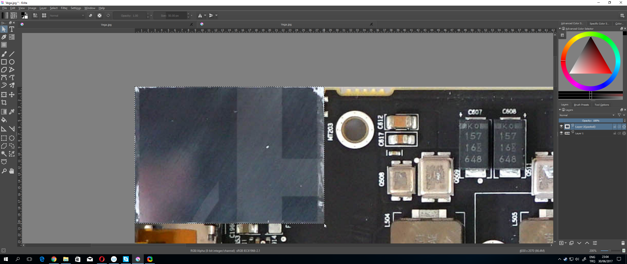
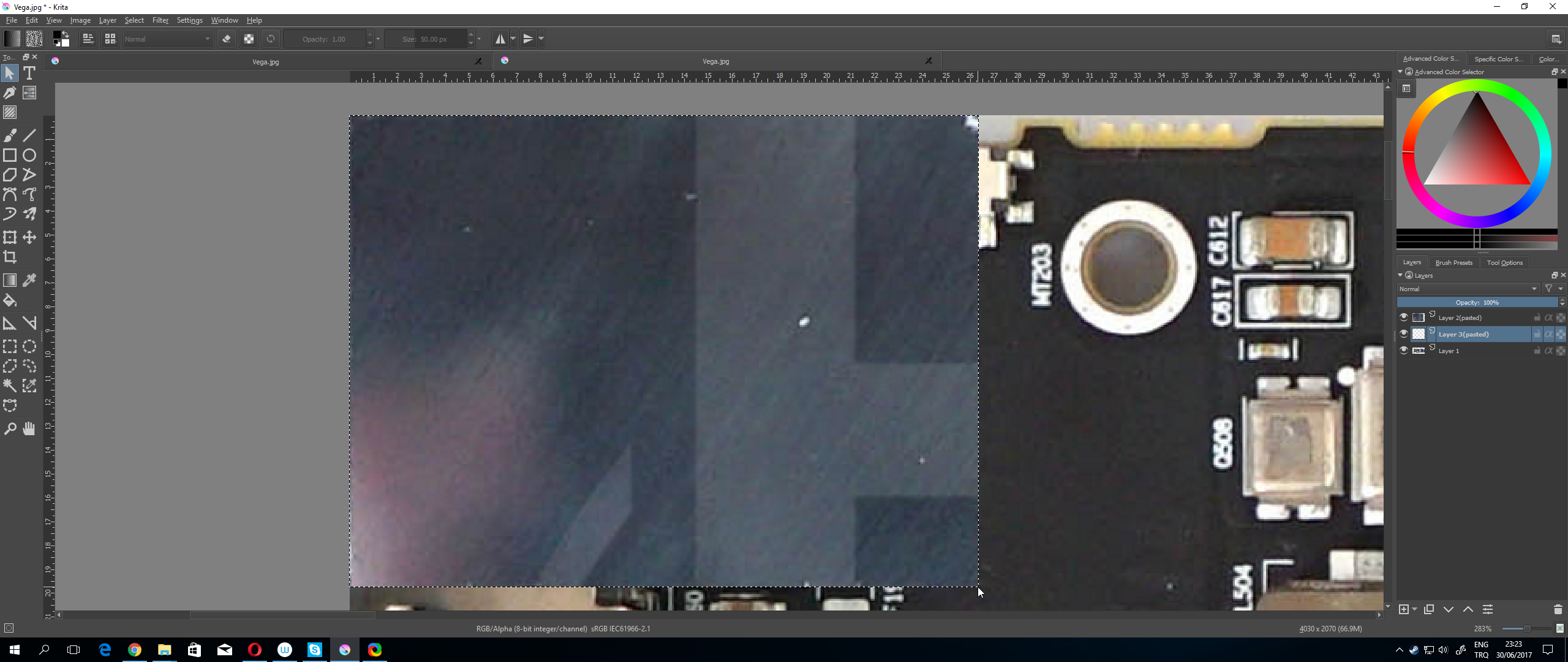
The marked rectangle in your last picture includes quite a bit more than just the GPU die on the sides.I placed the photo in Krita, resized the card to line up with the ruler at 267mm, and the chip looks to be about 28mm by 20mm putting it at 560mm^2.


PCPer's measurement appears to be accurate.
Edit: it's about 1.7mm too wide and a few pixels too high, which would make it 26.3 x 19.9 or something.
Edit2:
Taking the alleged 47.3mm x 47.3mm for the package, I arrive at 25.6mm x 19.4mm (rounded) = 498mm²
Last edited:
Why is the Fury X so efficient?
Why does it need so much power?
The marked rectangle in your last picture includes quite a bit more than just the GPU die on the sides.
Edit: it's about 1.7mm too wide and a few pixels to high, too, which would make it 26.3 x 19.9 or something.

Ok, second take. I revised the borders, which puts it around 26.25*19.75 = 518mm^2
It isn't a pixel perfect measurement but it should be more or less accurate. Maybe PCPer measured it wrong? Or maybe I measured it wrong?
Cache?Can that chip area be double-checked?
Fiji is 593mm2.
Kind of weird how close the area gets to Vega if it just "lost" two HBM interfaces. Where'd all the area savings from 14nm go?
We know the rest of the chip specs, so... ¯\_(ツ)_/¯
do we know if RX Vega is going to be using this same die? it seems hugely wasteful, massive increase in transistor count but hardly any efficiency gain for gaming compared to Fury X
this looks like a product that should be targeting the 1070 market at best based on performance, but with complexity/cost above the Titan Xp.... this might be more disappointing than the 2900XT was 10 years ago.
this looks like a product that should be targeting the 1070 market at best based on performance, but with complexity/cost above the Titan Xp.... this might be more disappointing than the 2900XT was 10 years ago.
Rootax
Veteran
Yeah, the most troubling thing for me is the power consumption. If performances were low like that, but the power consumption was more "normal", well, ok. But this... Something is broken somewhere, and I hope that reviewers will find what when RX Vega come out.
EDIT : "Funny" thing, if I want more performance (I've a Fury X right now, but in some game I hit vram limitation), Vega is the only way to go, since I've a Freesync display and I don't want to lose that. Maybe a better cooled Vega will have better consumption number, but, no review of the WC'ooled Vega FE yet...
EDIT : "Funny" thing, if I want more performance (I've a Fury X right now, but in some game I hit vram limitation), Vega is the only way to go, since I've a Freesync display and I don't want to lose that. Maybe a better cooled Vega will have better consumption number, but, no review of the WC'ooled Vega FE yet...
Written article for those allergic to video: http://www.gamersnexus.net/news-pc/2972-amd-vega-frontier-edition-tear-down-die-size-and-more
- 30mm x 30mm total size of interposer + GPU (does not include substrate)
- 20.25mm x ~26mm GPU die size
- 10mm x ~12mm HBM2 size (x2)
- ~4mm package height (this is the one that’s least accurate, but gives a pretty good ballpark)
- 64mm x 64mm mounting hole spacing (square, center-to-center)
- PCB ~1mm
D
Deleted member 13524
Guest
Something is clearly wrong.
Yes, something is very wrong either with Vega or PCPer's (p)review.
The chip is almost literally behaving like a Fiji with a 35% overclock. It apparently has the same amount of ALUs, TMUs and ROPs, yet it has almost 50% more transistors supposedly dedicated to getting higher IPC, but we're seeing none of that.
It's like everything that is new from Vega's arch is either disabled or broken.
PCPer's preview isn't without its fair share of twilight zone material, like the Fury X consuming 180W in some benchmarks.
Similar threads
- Replies
- 374
- Views
- 57K
- Replies
- 53
- Views
- 8K
- Replies
- 175
- Views
- 12K
- Replies
- 29
- Views
- 13K
- Replies
- 90
- Views
- 16K
