Xbox One (Durango) Technical hardware investigation

Status
Not open for further replies.
Funniest thing about all this is that most people just won't understand enough of the tech to declare a winner to the console wars. It was bound to happen eventually, but I'm still happy to see it.

But I want the console with more Gigahertz...to push more gigapixels..:mad:

It's all about untapped poowwaa....:LOL:
 
I don't see the point otherwise. If they claim something like that there has to be some truth to it.
Cell had a peak floating point processing power measured as about 180 GFlops, but it never maintained that. The triangle drawing performance of a GPU likewise can be measured as billions peak, but it never achieves that as the peak figure is only true if rendering unlit triangles. the 204 GB/s peak BW figure is dependent on some operational conditions which we don't understand, that renders the opportunity to get that peak BW as less than 100% (otherwise the bus would be listed as 204 GB/s, and not a min/max range). It may well be that the peak figure is only obtained in rather theoretical scenarios, like a GPUs peak triangle setup, and in reality the BW devs actually have available to use with the code they run is much lower. Or not, we don't know, but we do have suggestions that the real figure is around 133 GB/s.

This is meant to keep the heat down, and taking into account that the Xbox 360 suffered lots heat-related issues that cost dearly in the early days, that seems okay and the CPU can downclock the whole system -and itself- if the console struggles to dissipate heat.
That's for different operating modes. There's no way the XB1 can't cope with the heat of gaming, except maybe for rare cases where someone living in the dessert puts their XB1 under the window in full sun and games.

And it's the largest single chip to be made for a console launch.
Do we have any estimates for PS4's SoC?
 
Is the Xbox One DX 11.1+ or DX 11.2? On the Hotchips slides, it specifies DX 11.1+ but has been previously stated as DX 11.2 at the BUILD Conference. Conflicting information or different terminology?
 
With 2 billion transistors less, I'd guess it's pretty clear it'll be smaller?
Where do you get 2 billion less from? With 50% more GPU, the difference can't be that big, unless ESRAM either takes up 3 billion transistors, or the sound processor has a billion transistors (PS4's SoC incorporates similar components to XB1's regards decompression units etc., so we can't count MS's '15 processors' as completely additional, nor will they be large).

That said, this really isn't on topic. Other discussion has said ESRAM is denser so the die size might not be massively different (months ago I was suggesting PS4 would be cheaper to make due to smaller SoC, which was challenged), but it's pretty much a given XB1's SoC is the single largest chip to ever go into a console. It is less than the 500 mm^2 of PS3 though (can't find die sizes for XB360), which is where we have lost the monster console concept, but that's not to be unexpected. I wouldn't call 350 mm^2 tiny as BRiT did. ;)
 
Cell had a peak floating point processing power measured as about 180 GFlops, but it never maintained that.

Actually it was 230 GFlops theoretical, and Cell was one of the few processors that could actually achieve that sustained, partly thanks to its Ring bus and Local Store per SPE. Doesn't really change your point in this case though, just maybe not the best example. ;) More relevant is that very flew applications exist that would be only interested in getting the most GFlops out of the PS3's Cell processor.

but we do have suggestions that the real figure is around 133 GB/s.

This comes from a blend example that is a fairly optimal case for read-write ops in practice that is also used quite a lot in games.

Do we have any estimates for PS4's SoC?

Actually the size isn't that interesting. Last-gen chips were as big or bigger I think, thanks to the world then still being on 90nm tech. Transistor count is probably more interesting. The Xbox One chip is so large thanks to the 1.6 billion transistors or so for the on chip ESRAM. That leaves about 3.4 for all the other components. I think the PS4 chip is something like 4 billion transistors?

I'd like to see how long it would take this time for somebody to x-ray the Xbox one and PS4 SoCs.

Considering what happened with the Wii U, not long at all. The company that did it last time may do it for free this time just for PR.
 
...Cell was one of the few processors that could actually achieve that sustained, partly thanks to its Ring bus and Local Store per SPE. Doesn't really change your point in this case though, just maybe not the best example.
Every peak rating can be sustained in the right context. That Cell could hit its peak throughput yet only managed that a tiny amount of the time is precisely the point here. I've no doubt one could create a situation where XB1 gets 204 GB/s BW to/from the ESRAM, just as one could definitely get 25 GF/s from a SPE, but the actual amount of time that's obtained in an actual game environment will be minimal. The average throughput of Cell may be 25? 50? 100? GFlops (absolutely no idea!), but it certainly wasn't close to the peak rating, and the average BW on XB1 will likely be about 133 GB/s, maybe (we all have absolutely no idea!). The peak value is only an engineering concern, and not indicative of what the hardware actually achieves.
 
Funniest thing about all this is that most people just won't understand enough of the tech to declare a winner to the console wars. It was bound to happen eventually, but I'm still happy to see it.
This isn't much different from current gen, is it? :)

Is the Xbox One DX 11.1+ or DX 11.2? On the Hotchips slides, it specifies DX 11.1+ but has been previously stated as DX 11.2 at the BUILD Conference. Conflicting information or different terminology?
There aren't that many significant changes between the two (11.1 and 11.2 that is) to begin with. Mostly fast presents (which are cool) and tileable memory (which Carmack loves). My bet would be that 11.2 moniker could not be used prior to announcing its existence and presentations may be older or may reuse slides from older decks.
 
Is the Xbox One DX 11.1+ or DX 11.2? On the Hotchips slides, it specifies DX 11.1+ but has been previously stated as DX 11.2 at the BUILD Conference. Conflicting information or different terminology?
Most likely just old info. DirectX 11.2 was very recently announced. According to several gaming/tech web sites Microsoft has confirmed DX 11.2 support for Xbox One.

http://www.extremetech.com/gaming/1...xclusive-microsoft-dangles-the-upgrade-carrot

http://www.tomshardware.com/news/DirectX-11.2-Tiled-Resources-Xbox,23322.html

http://www.escapistmagazine.com/news/view/125435-Microsoft-Tiled-Resources-Key-To-Xbox-One-Graphics

http://venturebeat.com/2013/06/26/m...etailed-graphics-on-xbox-one-and-windows-8-1/
 
AMD has confirmed that both PS4 and XB1 APUs are DX11.2 capable, just like HD7 (and HD8 OEM) series
 
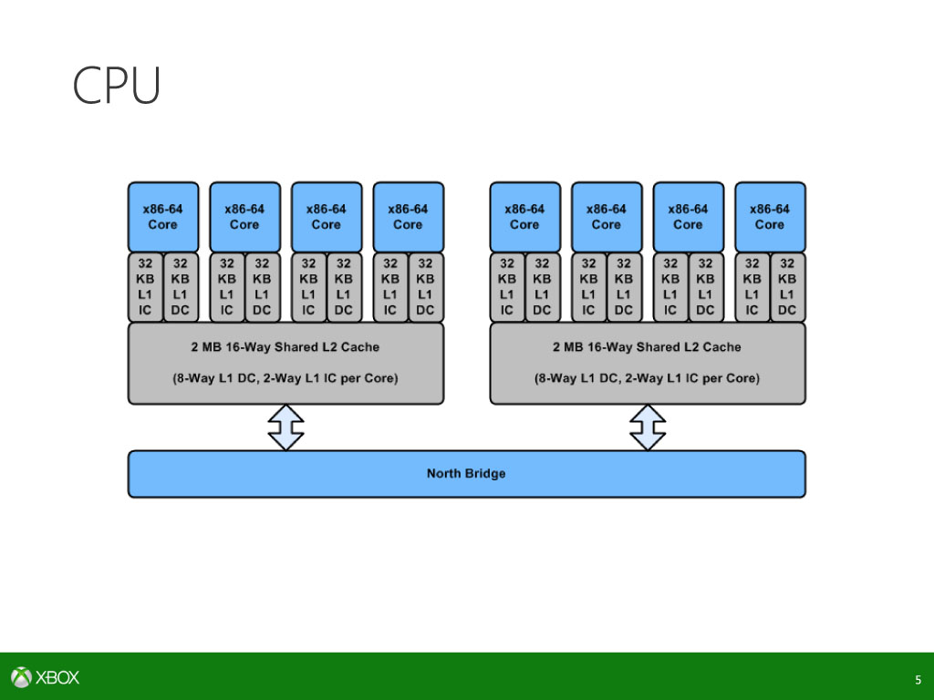
pc watch seems to have the best slides including the CPU (no clock, hardly anything)

http://pc.watch.impress.co.jp/docs/column/kaigai/20130827_612762.html


06.jpg
 
Last edited by a moderator:
I wouldn't call 350 mm^2 tiny as BRiT did. ;)

Its a large single chip for a console but not large compared to non-console chips. Its the same size area as the xbox360 launch CPU+GPU. Its going to be pad limited when shrunk down to the next micron mfg level due to the quad channel ddr3 interface and other io interfaces.
 
RV670 was 4x64bit GDDR3/4 on 55nm and just 192mm^2. Pad limitations are still a bit away I guess.


Also, consider the increased foundry wafer sizes compared to past console launches. Everyone across the board can afford larger diesizes at cheaper prices these days.
 
RV670 was 4x64bit GDDR3/4 on 55nm and just 192mm^2. Pad limitations are still a bit away I guess.

Right, but this is 4x256bit GDDR3 so you'll have substantially more pads.
 
Status
Not open for further replies.
Back
Top