For sure. I was just talking about how much it costs NVIDIA to have the chip manufactured.What I think a lot of people might not appreciate is the scale of those costs in relation to the amount of hardware sold, and the fact that all of those costs have to be spread across the number of products sold.
None of the IHVs really go into detail about this in their financials that I'm aware of, but just as a thought experiment...
Think about the complexity of the driver stack, the compiler, and then validation of the same, for something like a Riva TNT, an 8800GTX, and a 4090, and then think about the number of person-hours you'd need to develop, validate, and support the same.
Back in the early days, there wasn't even hardware video encode/decode to worry about, let alone GPGPU programming stacks, DLSS, all the effort put into making sure that shader compilation a) works and b) is performant, etc.
That all costs a ton of money at a scale that just wasn't the case back in the day. Even in a theoretical world where the cost of the silicon die was zero, or at least stayed the same each generation, all of those other costs have increased dramatically and would result in the cost of the product to the consumer necessarily being more expensive in order to have a viable business and keep the lights on.
There's certainly some argument to be made about the shape of that trend line, whether it's mostly linear, exponential, or somewhere in between, but you'd be hard pressed to argue that it does anything but increase each generation.
Install the app
How to install the app on iOS
Follow along with the video below to see how to install our site as a web app on your home screen.
Note: This feature may not be available in some browsers.
You are using an out of date browser. It may not display this or other websites correctly.
You should upgrade or use an alternative browser.
You should upgrade or use an alternative browser.
Cost of advanced chip manufacture
- Thread starter IQandHDR
- Start date
I was also talking mostly about the cost per die, which is greater than just the wost of a wafer as far as i can see.I think we're just talking about the cost of the die. Well that's what I'm talking about.
But alas a die does not make a graphics card.
Yeah, costs go up fast.What I think a lot of people might not appreciate is the scale of those costs in relation to the amount of hardware sold, and the fact that all of those costs have to be spread across the number of products sold.
None of the IHVs really go into detail about this in their financials that I'm aware of, but just as a thought experiment...
Think about the complexity of the driver stack, the compiler, and then validation of the same, for something like a Riva TNT, an 8800GTX, and a 4090, and then think about the number of person-hours you'd need to develop, validate, and support the same.
Back in the early days, there wasn't even hardware video encode/decode to worry about, let alone GPGPU programming stacks, DLSS, all the effort put into making sure that shader compilation a) works and b) is performant, etc.
That all costs a ton of money at a scale that just wasn't the case back in the day. Even in a theoretical world where the cost of the silicon die was zero, or at least stayed the same each generation, all of those other costs have increased dramatically and would result in the cost of the product to the consumer necessarily being more expensive in order to have a viable business and keep the lights on.
There's certainly some argument to be made about the shape of that trend line, whether it's mostly linear, exponential, or somewhere in between, but you'd be hard pressed to argue that it does anything but increase each generation.
But it doesn't help that the cost per transistor is not going down with each new process node.
Add the layers of complexcity on top of that i do not think we are talking about a linear scaling in cost, far from it.
I really liked this video as it helped me much better understand what a GPU today does:
They have really become complex with not just shader cores, but also tensor cores, RT cores etc.
Cost of transistor will be cost of die production divided by number of transistors. Cost of GPU is something else.Then there is R&D cost, memory cost, PCB cost, cooling, packaging and validation costs, .... etc.
More Moderatiously: This is a thread to attempt to identify the cost of a transistor. This can be computed as the cost to produce a working die divided by the number of transistors, or a more understandable variation (as 0.000000000231 cents isn't particularly user-friendly). The cost to produce a GPU or graphics card is a different discussion.
While the PDF is a few years old, it does contain data down to TSMC's 5nm node, which 4N is a derivative of, so should be fairly applicable to the historical comparisons in this thread: https://cset.georgetown.edu/wp-content/uploads/AI-Chips—What-They-Are-and-Why-They-Matter-1.pdf
In particular, pages 44/45 where it goes into the wafer costs and cost per chip (assuming the same # of transistors) for each node.
5nm definitely costs more per transistor and per chip produced than 7nm. One caveat - the PDF is fairly AI focused, and it looks like it's using the theoretical 'logic density' for its scaling factors between nodes, which is the absolute best case scenario and unlikely to actually be achieved in real world designs. You can see on page 41 they're assuming a ~78% density improvement between 7nm and 5nm.
SRAM and I/O in particular are still a significant chunk of a modern GPU and those scale much worse than the theoretical 'best case' scaling factors advertised by the fabs. The actual density improvement of high density SRAM cells from 7nm to 5nm is less than 30%, a far cry from the 78% assumed by the AI chips PDF, and even then they came to the conclusion that 5nm would cost more per transistor than 7nm.

 fuse.wikichip.org
In particular, pages 44/45 where it goes into the wafer costs and cost per chip (assuming the same # of transistors) for each node.
5nm definitely costs more per transistor and per chip produced than 7nm. One caveat - the PDF is fairly AI focused, and it looks like it's using the theoretical 'logic density' for its scaling factors between nodes, which is the absolute best case scenario and unlikely to actually be achieved in real world designs. You can see on page 41 they're assuming a ~78% density improvement between 7nm and 5nm.
SRAM and I/O in particular are still a significant chunk of a modern GPU and those scale much worse than the theoretical 'best case' scaling factors advertised by the fabs. The actual density improvement of high density SRAM cells from 7nm to 5nm is less than 30%, a far cry from the 78% assumed by the AI chips PDF, and even then they came to the conclusion that 5nm would cost more per transistor than 7nm.

IEDM 2022: Did We Just Witness The Death Of SRAM?
IEDM 2022: Did we just witness the death of SRAM? While foundries continue to show strong logic transistor scaling, SRAM scaling has completely collapsed.
 fuse.wikichip.org
Those numbers tell a boit of the "tale":While the PDF is a few years old, it does contain data down to TSMC's 5nm node, which 4N is a derivative of, so should be fairly applicable to the historical comparisons in this thread: https://cset.georgetown.edu/wp-content/uploads/AI-Chips—What-They-Are-and-Why-They-Matter-1.pdf
In particular, pages 44/45 where it goes into the wafer costs and cost per chip (assuming the same # of transistors) for each node.
5nm definitely costs more per transistor and per chip produced than 7nm. One caveat - the PDF is fairly AI focused, and it looks like it's using the theoretical 'logic density' for its scaling factors between nodes, which is the absolute best case scenario and unlikely to actually be achieved in real world designs. You can see on page 41 they're assuming a ~78% density improvement between 7nm and 5nm.
SRAM and I/O in particular are still a significant chunk of a modern GPU and those scale much worse than the theoretical 'best case' scaling factors advertised by the fabs. The actual density improvement of high density SRAM cells from 7nm to 5nm is less than 30%, a far cry from the 78% assumed by the AI chips PDF, and even then they came to the conclusion that 5nm would cost more per transistor than 7nm.

IEDM 2022: Did We Just Witness The Death Of SRAM?
IEDM 2022: Did we just witness the death of SRAM? While foundries continue to show strong logic transistor scaling, SRAM scaling has completely collapsed.fuse.wikichip.org

Thanks for the info
Can someone explain how they conclude a higher cost per transistor when the table above shows a drop in sale price per chip? Are they considering a fixed chip size in all nodes, not accounting for foundry clients using all the margin available for larger chips?
The final entry, for 5nm, the chip price does actually go up, very slightly.Can someone explain how they conclude a higher cost per transistor when the table above shows a drop in sale price per chip? Are they considering a fixed chip size in all nodes, not accounting for foundry clients using all the margin available for larger chips?
Their assumed scaling factors are wildly optimistic even for pure logic (which a GPU is not), and even for those they still came to the conclusion that a 5nm chip costs more from the fab than a 7nm one.
Even for pure logic, with no SRAM or analog I/O, 7nm to 5nm scaling is closer to 1.52x than the 1.78x they assume:
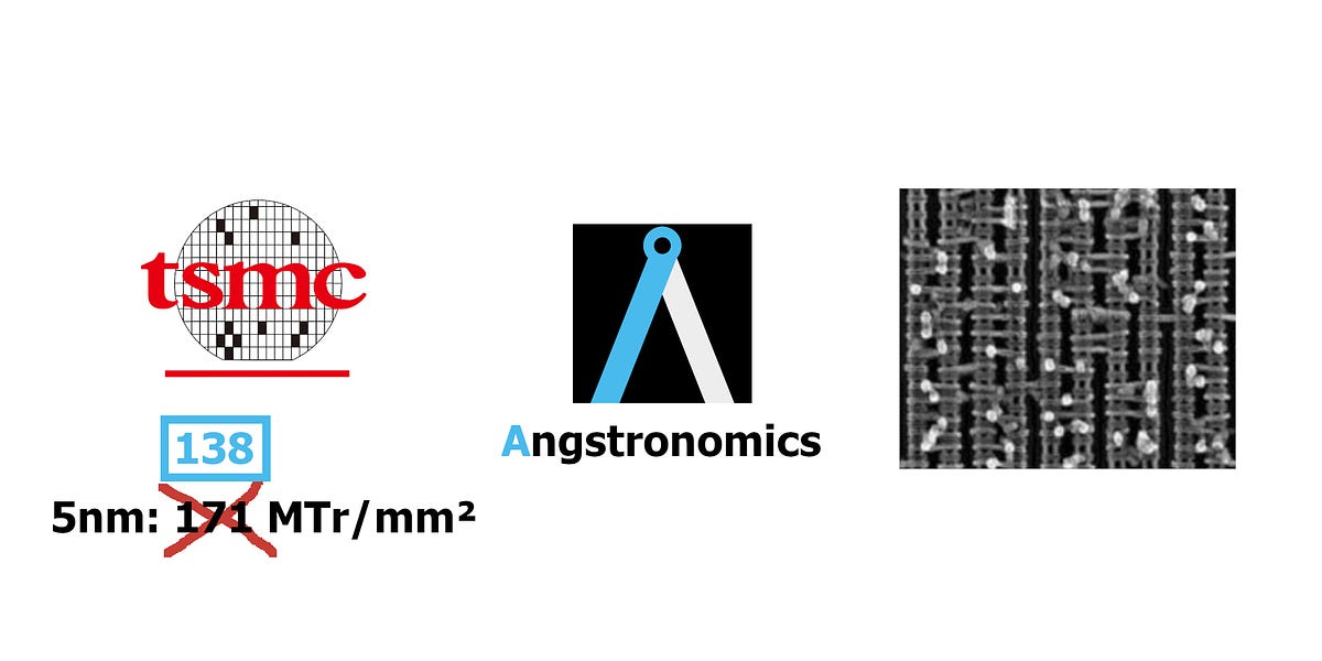
Another thing to consider is that the Fmax for the ADxxx series of GPUs went through the roof, by at least 40% and perhaps a bit more. Most Ada Lovelace GPUs will happily hit somewhere in the 2.8 -> 3.05ghz range out of the box versus previous generations hovering around 2.00ghz-ish. There's speculation that part of the secret sauce of what makes '4N' custom is use of the HP cell libraries like the 3-fin transistors as described in the Angstronomics article above. Great for hitting higher clock speeds, but they are physically larger and that hurts density even more, even for pure logic.
TSMC makes this really easy to see visually with their 3nm FinFlex slides, and desktop GPUs so far as I know tend to lean towards performance above all.

Ada Lovelace (microarchitecture) - Wikipedia
The overall density in the Wikipedia article listed there for the AD-series GPUs is significantly less than even the more pessimistic numbers in the Angstronomics article. Whether that's because of the SRAM and analog blocks bringing the number down, the use of HP cells, or a combination of both, is hard to say, but at the end of the day that makes the chip bigger and more costly.
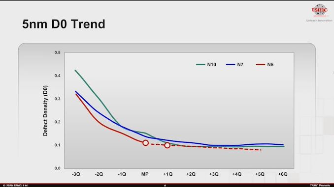
TSMC's defect density is somewhat known (Not exact figures of course but a ball park). TSMC claimed that N5 was doing better than N7 and we know it is below 0.1 at this point. You can input this into a yield calculator and get a fair idea of the likely yield (Not accounting for how much redundancy is built into the chip or usage of salvage parts naturally). Taking AD102 as 609mm2 and assuming a square die of 25*24.4 mm, defect density of 0.09 (This is conservative, from what I have read it is closer to 0.06 for long term mass production) and leaving all other parameters at defaults, I get a yield of 59% for AD102 for 0 defect chips - https://isine.com/resources/die-yield-calculator/BTW that puts AD102 at just over $200. But it could be more since more of the wafer is wasted on the edge (maybe yields are lower too). I'm sure the edge waste math is doable but not by me. And I don't know the yields.
-
I acutally think it is even more complicated than that:

Die Size And Reticle Conundrum – Cost Model With Lithography Scanner Throughput
Smaller Chiplets Isn’t Always BetterWe have been spending a lot of time in our private consulting business trying to build out a model of semiconductor fab capital expenditures by tool type f…semianalysis.com
View attachment 12420
I presume these come on top of the "bare" wafer cost.
The bare wafer cost is quite low, like ~$100 but this does not seem to account for R&D and capex, nor gross margin, which is ~50-55% at TSMC. The actual figures are of course proprietary and bound by NDAs so we can only speculate based on the table 9 figures linked.
While the PDF is a few years old, it does contain data down to TSMC's 5nm node, which 4N is a derivative of, so should be fairly applicable to the historical comparisons in this thread: https://cset.georgetown.edu/wp-content/uploads/AI-Chips—What-They-Are-and-Why-They-Matter-1.pdf
In particular, pages 44/45 where it goes into the wafer costs and cost per chip (assuming the same # of transistors) for each node.
5nm definitely costs more per transistor and per chip produced than 7nm. One caveat - the PDF is fairly AI focused, and it looks like it's using the theoretical 'logic density' for its scaling factors between nodes, which is the absolute best case scenario and unlikely to actually be achieved in real world designs. You can see on page 41 they're assuming a ~78% density improvement between 7nm and 5nm.
SRAM and I/O in particular are still a significant chunk of a modern GPU and those scale much worse than the theoretical 'best case' scaling factors advertised by the fabs. The actual density improvement of high density SRAM cells from 7nm to 5nm is less than 30%, a far cry from the 78% assumed by the AI chips PDF, and even then they came to the conclusion that 5nm would cost more per transistor than 7nm.

IEDM 2022: Did We Just Witness The Death Of SRAM?
IEDM 2022: Did we just witness the death of SRAM? While foundries continue to show strong logic transistor scaling, SRAM scaling has completely collapsed.fuse.wikichip.org
True, one of the factors which has caused chip costs to go up significantly is the slowdown in scaling since 7nm, particularly for SRAM, and this trend is getting worse with 3nm and beyond. And as mentioned, chip designs use different libraries for different parts of the chip depending on if they are targeting higher performance or lower area, can spend transistors on dark silicon/redundancy, etc so naturally getting a true picture of cost per transistor is always going to be rather difficult based on publicly available information. The general trends have been that cost per transistor have been increasing since 28nm and are likely to accelerate even further with 2nm and beyond. A minor point to keep in mind is DRAM cost scaling has also slowed down and this has also contributed to the increase in cost for GPUs in particular.
The increase of transistor from Ampere to Ada Lovelace is still mindboggling to me:The overall density in the Wikipedia article listed there for the AD-series GPUs is significantly less than even the more pessimistic numbers in the Angstronomics article. Whether that's because of the SRAM and analog blocks bringing the number down, the use of HP cells, or a combination of both, is hard to say, but at the end of the day that makes the chip bigger and more costly.
Code:
GA102-350-A1    Transistors (Billion) 28.3 Die: 628.4 mm2 Cache:  6 MiB
AD102-300       Transistors (Billion) 76.3 Die: 608.5 mm2 Cache: 72 MiB
The cache going up +12x holds some of the explanation I think.
Do you know if lithographing memory (if that is even a word) is more or less expensive than lithographing logic?
I presume not all transistors are created equally?
TSMC's defect density is somewhat known (Not exact figures of course but a ball park). TSMC claimed that N5 was doing better than N7 and we know it is below 0.1 at this point. You can input this into a yield calculator and get a fair idea of the likely yield (Not accounting for how much redundancy is built into the chip or usage of salvage parts naturally). Taking AD102 as 609mm2 and assuming a square die of 25*24.4 mm, defect density of 0.09 (This is conservative, from what I have read it is closer to 0.06 for long term mass production) and leaving all other parameters at defaults, I get a yield of 59% for AD102 for 0 defect chips - https://isine.com/resources/die-yield-calculator/
-
The bare wafer cost is quite low, like ~$100 but this does not seem to account for R&D and capex, nor gross margin, which is ~50-55% at TSMC. The actual figures are of course proprietary and bound by NDAs so we can only speculate based on the table 9 figures linked.
True, one of the factors which has caused chip costs to go up significantly is the slowdown in scaling since 7nm, particularly for SRAM, and this trend is getting worse with 3nm and beyond. And as mentioned, chip designs use different libraries for different parts of the chip depending on if they are targeting higher performance or lower area, can spend transistors on dark silicon/redundancy, etc so naturally getting a true picture of cost per transistor is always going to be rather difficult based on publicly available information. The general trends have been that cost per transistor have been increasing since 28nm and are likely to accelerate even further with 2nm and beyond. A minor point to keep in mind is DRAM cost scaling has also slowed down and this has also contributed to the increase in cost for GPUs in particular.
So ~40 usesable dies for AD102 per wafer or I am not reading your post correctly?
And should one add the cost of defective (wasted transistors) dies to the combined cost of healthy dies?
Because that would make the "cost per transistor" go up quite a bit just on it own.
arandomguy
Veteran
That would be dies without any defects and not yields of final products. RTX 4090 as configured already allows for defects. We also don't know how much redundancy and dark silicon is inherently built into GA102 which would also mitigate defects.
The other aspect of this to consider is parametric yield loss. That is there isn't a physical defect but certain chips (or part of chips) cannot meet the power/performance requirements specs for final products.
The other aspect of this to consider is parametric yield loss. That is there isn't a physical defect but certain chips (or part of chips) cannot meet the power/performance requirements specs for final products.
Ah yes, I as understand it it the AD102-300 (RTX 4090) is 87.5% of a full AD120 die.That would be dies without any defects and not yields of final products. RTX 4090 as configured already allows for defects. We also don't know how much redundancy and dark silicon is inherently built into GA102 which would also mitigate defects.
The other aspect of this to consider is parametric yield loss. That is there isn't a physical defect but certain chips (or part of chips) cannot meet the power/performance requirements specs for final products.
And the AD102-175-KEF-A1 (RTX 4070 Ti Super) is 45.8% of a full AD102 die. (just found this on google)
So some dies are apparently less than 50% functional on AD102...no I just wonder how even more on the defect rates

The increase of transistor from Ampere to Ada Lovelace is still mindboggling to me:
Code:GA102-350-A1 Transistors (Billion) 28.3 Die: 628.4 mm2 Cache: 6 MiB AD102-300 Transistors (Billion) 76.3 Die: 608.5 mm2 Cache: 72 MiB
The cache going up +12x holds some of the explanation I think.
Do you know if lithographing memory (if that is even a word) is more or less expensive than lithographing logic?
I presume not all transistors are created equally?
Ampere was on Samsung "8nm", a derivative of their 10nm process, which itself was a derivative of 14nm vs Ada which is on TSMC "4nm" so we're already comparing between 2 different fabs altogether. There is a full node jump between 14/16nm to 7nm and then 7nm to 5/4nm so the difference in density is largely due to an almost 2 node jump (which is historically a rough doubling of density), which is atypical. And yes the large increase in cache is another reason. Cache is denser than logic which is denser than analog, so in mm2 terms, cache is cheaper per transistor (and even cache can use different libraries). The proportion of analog in the AD102 die is also presumably less vs GA102 as the memory interface and technology have remained largely the same so that would also account for an overall increase in density.
So ~40 usesable dies for AD102 per wafer or I am not reading your post correctly?
And should one add the cost of defective (wasted transistors) dies to the combined cost of healthy dies?
Because that would make the "cost per transistor" go up quite a bit just on it own.
48 good dies per wafer from the link I posted but that does not take into account redundancy, salvageability, parametric yields as mentioned by @arandomguy. If I take another calculator I get 50 dies so it's in the same range - http://cloud.mooreelite.com/tools/die-yield-calculator/index.html

However, this is very simplistic and there are many more optimizations you can make including die shape, redundancy, product planning/salvageability to maximize use of chips.
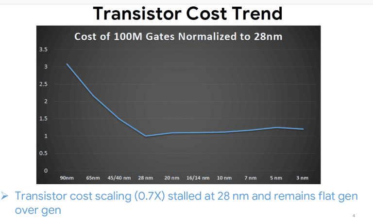
This is not an accurate method to measure or compare cost per transistor though. The basic cost per transistor itself can vary depending on type of transistor, i.e. logic, sram, analog, not accounting for differences in libraries and design. TSMC for example uses a mix of 50% logic, 30% SRAM and 20% analog when it makes chip density comparisons between nodes in it's marketing materials. Assuming that the publishers of the below chart have used some variation of this, it would give you a fair idea of the relative production cost per transistor, without taking into account all of the other costs mentioned, i.e. design, IP, verification, testing, mask costs, etc. In general, it seems that the cost per transistor is increasing gen on gen since 28nm.
Last edited:
Ampere was on Samsung "8nm", a derivative of their 10nm process, which itself was a derivative of 14nm vs Ada which is on TSMC "4nm" so we're already comparing between 2 different fabs altogether. There is a full node jump between 14/16nm to 7nm and then 7nm to 5/4nm so the difference in density is largely due to an almost 2 node jump (which is historically a rough doubling of density), which is atypical. And yes the large increase in cache is another reason. Cache is denser than logic which is denser than analog, so in mm2 terms, cache is cheaper per transistor (and even cache can use different libraries). The proportion of analog in the AD102 die is also presumably less vs GA102 as the memory interface and technology have remained largely the same so that would also account for an overall increase in density.
48 good dies per wafer from the link I posted but that does not take into account redundancy, salvageability, parametric yields as mentioned by @arandomguy. If I take another calculator I get 50 dies so it's in the same range - http://cloud.mooreelite.com/tools/die-yield-calculator/index.html
View attachment 12424
However, this is very simplistic and there are many more optimizations you can make including die shape, redundancy, product planning/salvageability to maximize use of chips.
This is not an accurate method to measure or compare cost per transistor though. The basic cost per transistor itself can vary depending on type of transistor, i.e. logic, sram, analog, not accounting for differences in libraries and design. TSMC for example uses a mix of 50% logic, 30% SRAM and 20% analog when it makes chip density comparisons between nodes in it's marketing materials. Assuming that the publishers of the below chart have used some variation of this, it would give you a fair idea of the relative production cost per transistor, without taking into account all of the other costs mentioned, i.e. design, IP, verification, testing, mask costs, etc. In general, it seems that the cost per transistor is increasing gen on gen since 28nm.
Thank you for the insights, this area is more complex than I first assumed and I value your inputs.
Makes me wonder how low consumers can keep up with the costs (eg. GPU users) since this indicates for me that cost will soon spiral upwards fast...and private consumers does not have the same "deep pockets" as enterprise and the A.I. industry seems to a VERY deep pockets atm.
I guess the only conclusion we can drwas without more specific numbers are that the cost per transistor is indeed increasing since 28nm and this increase will not be linear, but accelerate in the near future.
You're welcome, it is indeed a lot more complex than just comparing die sizes and transistor counts, without going further into economic and financial calculations as well.
If you see the recent trend, it is one where prices of consumer hardware have in general been going up (there are exceptions but for chips using newer nodes it's largely true), though this is also due to inflation as well. There are many ways to mitigate this. Except for flagship mobile SoCs and high end PC/mobile chips, in the recent past mainstream consumer hardware has been using trailing node(s), for both cost and volume reasons. We have also seen Nvidia for example reducing the die size of certain tiers of chips gen on gen to keep costs in check, and AMD using chiplets to keep some tiles on leading edge nodes and others on older, more cost effective nodes. The cost of nodes also goes down later in the lifecycle once the equipment is depreciated (typically 4-5 years from start of mass production). Use of higher power limits also allows for higher performance at the expense of power consumption, which is more tolerable on consumer hardware than enterprise/AI. Mainstream consumer hardware is likely to continue using a combination of these factors to keep costs in check, though a minor cost increase year on year is also likely.
In general yes, this is due to use of new technologies and transistor types, increasing fab capex and one factor not really mentioned is reduced competition where TSMC largely has pricing power.
Last edited:
You're welcome, it is indeed a lot more complex than just comparing die sizes and transistor counts, without going further into economic and financial calculations as well.
If you see the recent trend, it is one where prices of consumer hardware have in general been going up (there are exceptions but for chips using newer nodes it's largely true), though this is also due to inflation as well. There are many ways to mitigate this. Except for flagship mobile SoCs and high end PC/mobile chips, in the recent past mainstream consumer hardware has been using trailing node(s), for both cost and volume reasons. We have also seen Nvidia for example reducing the die size of certain tiers of chips gen on gen to keep costs in check, and AMD using chiplets to keep some tiles on leading edge nodes and others on older, more cost effective nodes. The cost of nodes also goes down later in the lifecycle once the equipment is depreciated (typically 4-5 years from start of mass production). Use of higher power limits also allows for higher performance at the expense of power consumption, which is more tolerable on consumer hardware than enterprise/AI. Mainstream consumer hardware is likely to continue using a combination of these factors to keep costs in check, though a minor cost increase year on year is also likely.
In general yes, this is due to use of new technologies and transistor types, increasing fab capex and one factor not really mentioned is reduced competition where TSMC largely has pricing power.
Indeed, the complexity surprised me and I work in enterrpise IT
I didn't even factor in TSMC profit margins,so while I knew the cost was not decreasing anymore, I did not know a lot of the factors, so it has been very iluminating to get all these insights...and a bit weary as a future consumer.
I "learned" a lot in a short time, so I am a "happy camper" right now
DavidGraham
Veteran
Speaking of which, TSMC just raised prices for all nodes again this year.didn't even factor in TSMC profit margins
Previous they hiked prices by as much as 8% for all nodes.

TSMC To Raise 3nm & 5nm Prices By Up To 8%, CoWoS To Witness Price Increase Too
TSMC is set to implement a "price raise" strategy across its in-demand products since the Taiwan giant is eager to maintain its gross margins.
They are also planning a third price hike further into 2025 for all nodes (by 10%).
TSMC to Raise Wafer Prices by 10% in 2025, Customers Seemingly Agree
Taiwanese semiconductor giant TSMC is reportedly planning to increase its wafer prices by up to 10% in 2025, according to a Morgan Stanley note cited by investor Eric Jhonsa. The move comes as demand for cutting-edge processors in smartphones, PCs, AI accelerators, and HPC continues to surge...
Speaking of which, TSMC just raised prices for all nodes again this year.
Previous they hiked prices by as much as 8% for all nodes.

TSMC To Raise 3nm & 5nm Prices By Up To 8%, CoWoS To Witness Price Increase Too
TSMC is set to implement a "price raise" strategy across its in-demand products since the Taiwan giant is eager to maintain its gross margins.wccftech.com
They are also planning a third price hike further into 2025 for all nodes (by 10%).

TSMC to Raise Wafer Prices by 10% in 2025, Customers Seemingly Agree
Taiwanese semiconductor giant TSMC is reportedly planning to increase its wafer prices by up to 10% in 2025, according to a Morgan Stanley note cited by investor Eric Jhonsa. The move comes as demand for cutting-edge processors in smartphones, PCs, AI accelerators, and HPC continues to surge...www.techpowerup.com
Keep in mind TSMC's largest customers such as Apple, Nvidia, AMD, Qualcomm, etc all sign long term wafer supply agreements with negotiated prices years in advance. The price hikes to their list prices will not have a major impact in the near term, except for those looking for additional capacity or new customers. Part of the price increase is also due to general inflation and supply chain issues.
It will make more of a difference in the medium to long term when it comes to renewing the agreements or negotiating new agreements. TSMC is signaling and have pretty much stated as much that they want to take their gross margins up further. Unfortunately for the rest of the industry neither Samsung nor Intel have been able to be competitive enough to offer a credible alternative.
So another factor driving up cost that is not directly related to pure manufactoring cost.Keep in mind TSMC's largest customers such as Apple, Nvidia, AMD, Qualcomm, etc all sign long term wafer supply agreements with negotiated prices years in advance. The price hikes to their list prices will not have a major impact in the near term, except for those looking for additional capacity or new customers. Part of the price increase is also due to general inflation and supply chain issues.
It will make more of a difference in the medium to long term when it comes to renewing the agreements or negotiating new agreements. TSMC is signaling and have pretty much stated as much that they want to take their gross margins up further. Unfortunately for the rest of the industry neither Samsung nor Intel have been able to be competitive enough to offer a credible alternative.
It seems to me that all factors are going up in price, so price per transistors are only going one way

Similar threads
- Replies
- 34
- Views
- 7K
- Replies
- 21
- Views
- 4K
- Replies
- 75
- Views
- 15K
D
- Replies
- 70
- Views
- 22K
- Replies
- 188
- Views
- 35K
