Sounds like a wish from nintendo fan
huh?
Follow along with the video below to see how to install our site as a web app on your home screen.
Note: This feature may not be available in some browsers.
Sounds like a wish from nintendo fan
http://www.tomshardware.com/news/Pitcairn-radeon-HD-7850-768-shaders-gpu,15524.html
+
AMD A10
= 1152 Shaders.
Sound familiar?
Coupled with the Sweetvar's comments about Orbis/Durango going with equivalent of market's 7700/7800 series GPUs for the dev kits...
Arthur Gies from polygon.com posting some very interesting posts on neogaf .
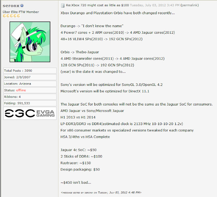
Interesting. Putting together all the rumors (e.g the pastebin one, the 16 "cores" one), this what I get:
8 Jaguar core @ 1.6 Ghz = 100 Gigaflops
8 CUs @ 1 Ghz = 1 Teraflop/s
Differently from an APUs, MS could have stripped down everything not needed (TMU, ROPs, tessellation unit), and using the CUs as huge FPU, with improved caches and other compute-related features. In some way it's what the Cell was build for, but way easier to code.
Even if they use a Cape Verde-like chip as dedicated GPU, we still have a fairly powerful console.
http://www.tomshardware.com/news/Pitcairn-radeon-HD-7850-768-shaders-gpu,15524.html
+
AMD A10
= 1152 Shaders.
Sound familiar?
Coupled with the Sweetvar's comments about Orbis/Durango going with equivalent of market's 7700/7800 series GPUs for the dev kits...
A Pitcairn derivative in a one slot card could only mean: console with updatable graphics.
I think bkilians recent post was a good nix on why this concept is a bad idea.
If anyone would do it (APU+discrete) I see Sony. Simply because they tend to embrace weird esoteric, not necessarily efficient designs, and it would be somewhat of a follow up conceptually to Cell. But hell now that Kutaragi is gone and the way Vita looks (very traditional) who even knows if they do that anymore.
Pretty sure the final console will have the apu and gpu combined into one big apu with aggregate performance north of 2 teraflops and 2-4 gigs of unified ultra fast ram.
If "final" means years from launch with smaller processes, maybe, but on launch no chance. MCM could in theory be feasible, but single die? No way it would be too big and controlling hotspots get too hard, I believe.
Why? Pitcairn has 2.5 TF on a 212mm^2 die @ 175W. 8 Jaguar cores and 4MB of cache for them are like >40mm^2 extra. A 250mm^2 die is eminently manufacturable, and if you disable 2 CUs for yields and drop the clocks to 900MHz, you are still above 2TF but now probably at 150W. That's right on the upper limit of feasible, but I think it's still within it.
Personally, I'd bet for a smaller system, but I don't think that's absurd.
You forgot the GPU of the APU from that equation, since the premise was APU + GPU on single die
--
fehu, I'd imagine it's easier to balance 2 separate dies hotspots than 1 big die with CPU cores, GPU cores and bigger set of GPU cores on it
(the APU+GPU rumor would support one rumor that said that there will be GPGPU heavily involved, but it won't be the "discrete GPU" doing that job)
Where is the source of the APU+GPU rumor? I've always though the dev kits are APU+GPU out of necessity.
Sweetvar started out saying the Orbis would be an APU solution.
I'm not quite sure, but I think somewhere it was suggested that the final would be APU (CPU + GPU for GPGPU) + GPU (graphics)
sweetvar26 said:The PS4 AMD project called as Thebe. Previously it used to be based on Themesto and Callisto based chips but now that has been revised. They moved on to a chip called Jaguar replacing the Streamroller. They moved on to TSMC 28nm solution from the 32, which the streamroller is.
The whole thing basically is APU solutuion, they made the changes considering the 10 year product life cycle and to keep the initial product costs at minimum. , As of now it is called as the Thebe Jaguar project or TH-J.
sweetvar26 said:As of what I've talked to him or heard, though they are doing project on the PS4 as well as the next Xbox, supposedly the Xbox project is on higher priority compared the PS4 and that they are developing something unique for it.
sweetvar26 said:Alright, I'm in Toronto and was talking to my buddy who works at the AMD headquarters here.
As of what he tells me, they both are using same chip with different specifications from Sony and Microsoft, something like the market's 7700-7800, not really sure. He did mention the word "Jaguar processor".
As for the PS4, the first chip has already been sent out two months ago, it is back after a month or so, for the second revision. He says there should be a third and if they don't see any problems, should be ready for mass production. Apparently, AMD did delay the work, he says it is around 6 months behind schedule.
sweetvar26 said:PS4:
New Starsha GNB 28nm TSMC
Milos
Southern Islands
DX11
SM 5.0
Open CL 1.0
Quad Pixel pipes 4
SIMD’s 5
Texture Units 5TCP/2TCC
Render back ends 2
Scalar ALU’s 320
EDIT: Some of those were crossed, may be they were updated/changed at a later date, I have no idea.
sweetvar26 said:PS4:
Couple of more updates
Graphic North Bridge(GNB) Highlights
Fusion 1.9 support
DCE 7.0
UVD 4.0
VCE
IOMMU
ACP
5x8 GPP PCIE cores
SCLK 800MHz/LCLK 800MHz
Nope. I think we're all thrown off track by dev kit specs.
Now that Sweetvar's info is confirmed to be legit (even his posts on Google Cache have been removed), his word is holy. All his words on Orbis so far.
There are also his posts on Starsha the early chipsets in PS4, but they've been wiped from the internet.

