Predict: The Next Generation Console Tech

Status
Not open for further replies.
That's how it's looking at the moment with what little info we have. Enhanced Memory Systems have their 'eSRAM' technology that is a 1T SRAM implementation. I can find reference to a 72Mb ESRAM component which matches the Wiki reference to the HP processor. That'd be 9 MBs. 9 MBs of local cache for a GPU? Why? But then Wii has 24 MBs 1T, so I expect we could be looking at a slightly less dense but much faster replacement for eDRAM, in theory.

That makes more sense as the quoted part has it as "ESRAM" and not "eSRAM". Could be just a bad interpretation on my part.
 
Perhaps, we'd be looking at something like 32-64MB of SRAM with a 1TB/sec bandwidth.

I'd like to point out that 64MB of SRAM would be 3B transistors, that is, basically all of the transistor budget the console would have.

64MB of 1T-SRAM, or eSRAM, would be equivalent of ~800M transistors or so, I don't actually have good density figures on a modern process for either. Personally, I'd bet for <50MB of the stuff, however, this time with the rops connected so that you can render both to the small pool and the large one. (The structure of modern AMD GPUs is inherently more flexible in how the rops connect to memory).
 
I figure I've sat on this tidbit long enough. It seems Xbox 3's final GPU will have eSRAM instead of eDRAM. I made sure to confirm eSRAM wasn't a misspelling. I don't know the amount though.

I should also add he clarified at that time that the "1+ TFLOP" was an estimate from someone else.

Interestingly the individual who said he had a couple sources specifically said (as I noted before) Durango had some "special" RAM that was not eDRAM (my older PM's got cut off on that forum but he mentioned it as recently as 7/28).

I wouldn't say this is a double confirmation, but I feel there are indications there may be some "unique" memory in Durango that is NOT eDRAM. Of course both of our sources could have the same root and be wrong...
 
64MB of 1T-SRAM, or eSRAM, would be equivalent of ~800M transistors or so, I don't actually have good density figures on a modern process for either. Personally, I'd bet for <50MB of the stuff, however, this time with the rops connected so that you can render both to the small pool and the large one. (The structure of modern AMD GPUs is inherently more flexible in how the rops connect to memory).

You'd probably be looking at <100mm^2 and it is something that'd be easy to merge into the main die at the first available shrink. You'd likely also get quite good yields out of it given it would be a relatively simple chip.

Would having ROPs etc embedded in RAM again be of any benefit to tessellation?

Yes, only 100mm^2. Roughly as big as the entire GPU itself if it's a Cape Verde. Nothing at all really!

And merging into the main die at first shrink didnt exactly work out for 360 now on something like it's 4th shrink and not merged (though, maybe you're implying this stuff would be different).

Anyways great info bg. Although of course it fits with the picture I've expected if we're talking about DDR3/4 as main memory.
 
Yes, only 100mm^2. Roughly as big as the entire GPU itself if it's a Cape Verde. Nothing at all really!

Pitcairn is ~ 75mm^2 per 1B transistors and I would presume they ought to be able to pack SRAM tighter than that on a more mature process with a simple structure.

And merging into the main die at first shrink didnt exactly work out for 360 now on something like it's 4th shrink and not merged (though, maybe you're implying this stuff would be different).

It uses the same process technology as the rest of the chip, it ought to be easier.
 
Thats a typical rubbish meaningless statement.
Explain then how in 9 months with no architectural changes you can go from bulldozer to piledriver if everything is so fundamentally broken ?

Also i guess you never owned a I7 920 C0 stepping like i do, on the stock cooler at stock 2.66ghz clock i could make it hit 100C and auto shutdown. I guess Nehalem was hot, slow and unfix-able :rolleyes:.

the problem with bigots is that when you dig any deeper then the generic label they get shiity real fast. No one is saying Orochi is a good product or you should put Orochi in a console so whats your point anyway?

and as bad as bulldozer is thats a complete lie.
heres some facts for your BS.
http://www.anandtech.com/bench/Product/49?vs=434
that is unless your favorite program in the world is sysmark 2007.

Ironic that you can have a spaz in another section of the forum for someone posting partisan ill considered rubbish then do the same in another section.

You sir seem to have a valid argument....the "other guy" not so much despite the dramatic knee jerk rant that is often just a cover/substitute for lack of true knowledge and comprehension.
 
660Ti uses 192 bit bus, yet there both 2GB and 3GB versions.

Couldn't this have implications for consoles? Memory amount not tied to bus width?
 
I'd like to point out that 64MB of SRAM would be 3B transistors, that is, basically all of the transistor budget the console would have.

64MB of 1T-SRAM, or eSRAM, would be equivalent of ~800M transistors or so, I don't actually have good density figures on a modern process for either. Personally, I'd bet for <50MB of the stuff, however, this time with the rops connected so that you can render both to the small pool and the large one. (The structure of modern AMD GPUs is inherently more flexible in how the rops connect to memory).

That's a lot. But, manufacturing an SRAM would be a lot easier than a processor of the equivalent size thanks to the uniformity. You can layout a very compact cell by hand and replicate that. The density should be really good.

I would guess that the physical size are would be about the same of the original eDRAM (75-100mm) and how much you can fit into that at 32/28nm so chances are 64-MB of 1T-SRAM would be doable, full SRAM probably not.

I just don't think ~8-10 MB would be enough, I think they need an increase over the 360 in both size and bandwidth.

Sure, but they dont necessarily need to go straight from 10mb to 64mb imo. I'd hope for something like 32mb to keep the tran budget reasonable.
 
Wouldn't 32 MB be quite sufficient? I guess 64 MBs is needed for 4xMSAA 16 bit per channel 1080p, but that's an awful lot of transistors for storage. If the main system BW is enough, it isn't really needed. As a working space, perhaps tiled rendering again, 32 MBs is plenty for rendering a buffer. Particle buffers that would need massive BW can get away with being quarter res or lower AA or somesuch compromise to fit a smaller buffer.
 
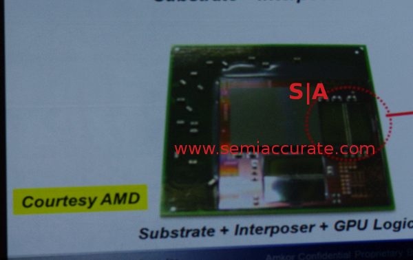
I keep thinking about the Interposer + GPU Logic that appeared on Semiaccurate a while ago and came from this presentation:

sites.amd.com/la/Documents/TFE2011_001AMC.pdf

Page 2 gives a pic of the prototype and timeline as end of 2013 for interposer, DDR, Logic.

Page 8 shows the chip as "Substrate + Interposer + GPU logic"

Interestingly it's "GPU logic", not GPU. Perhaps this is an early prototype of the new daughter die for the next Xbox.

Perhaps what we'll see is an APU consisting of 8 cores and 512-1024 shaders on one die, but the ROPS (and other logic that would make sense to put there ) on daughter die with 32MB of SRAM.

Effectively, you could say this would be just an evolution of the current 360 architecture..
 
are we talking MB or Mb here, i typo'd in my last post and said MB when i was thinking Mb......lol
Megabytes. 64 megabits would be 8MB - less than 360. We know 24 MB of 1T-SRAM exists on Wii, but do we know if it's on die or just on package? If on die, that bodes well for Durango. If on package, I fuess 16 to 32 MBs of 1T-SRAM would fit on a GPU die. If they go layered asMcHuj suggests, we've got no ideas what's possible!
 
For those interested I found a PDF on ESRAM on Google Patents.

http://www.ece.umd.edu/courses/enee759h.S2003/references/ss2615ds_r1.0c.pdf

I'm also working under the assumption that this info is ~10 years old and improvements would have obviously been made.

I guess EMS are using eSRAM to differentiate 1T-SRAM from normal SRAM?

Missed MrFox's post. But for the sake of accuracy it's probably best to use a capital E and not my erroneous usage of a lower case e.
 
Last edited by a moderator:
This was posted earlier this year. Seems like some kind of AMD GPU prototype, with stacked memory. Although I seriously doubt its from next gen console.

AMD_Interposer_SemiAccurate.jpg
 
Status
Not open for further replies.
Back
Top