Next Generation Hardware Speculation with a Technical Spin [post E3 2019, pre GDC 2020] [XBSX, PS5]

Status
Not open for further replies.
Looking at the benchmarks it appears to me the only card that's native 4k/60fps stable is 2080 ti (on current gen titles even), not even 2080 holds it that often and much less a 2070 tier console. The only games that are 4k/60 for a 2070 level ps5 are BF5 and Strange Brigade and the rest averages around 30-45fps.
https://www.guru3d.com/articles_pages/msi_geforce_rtx_2080_ti_lightning_z_review,13.html
Could it be a 4k cbr 60fps at max settings current gen beast? Most likely. But then what of next gen?

Framerate performance can also be affected by memory/bandwidth restrictions and/or storage drives that can't keep pace with streaming world assets (i.e., hitching, frame tearing, etc.). So, everything framerate related shouldn't always fall squarely on GPU and CPU performance metrics or benchmarks. If anything, we should start to see more solid/stable 60fps games (if the developers are aiming for such framerates) next-generation because of the reported SSD solutions and the possible rumored memory/bandwidth configurations. Just watch, the SSD solutions are going to be the biggest game changer. And of course the midrange Zen 2 Ryzen CPUs will definitely help towards better framerates.
 
Framerate performance can also be affected by memory/bandwidth restrictions and/or storage drives that can't keep pace with streaming world assets (i.e., hitching, frame tearing, etc.). So, everything framerate related shouldn't always fall squarely on GPU and CPU performance metrics or benchmarks. If anything, we should start to see more solid/stable 60fps games (if the developers are aiming for such framerates) next-generation because of the reported SSD solutions and the possible rumored memory/bandwidth configurations. Just watch, the SSD solutions are going to be the biggest game changer. And of course the midrange Zen 2 Ryzen CPUs will definitely help towards better framerates.

Yep, the general undersell of the impact of SSD is interesting.

With the old DayZ mod SSD gave a major boost to frame rates during built up areas and (I assume) the faster streaming of assets from the SSD vs HDD.

Nextgen will remove a lot of barriers for devs and frame rate issues.
 
I think the figures often center on the power cost of the interface itself, when discussed from the memory module's point of view. From a board perspective, there are elements like the memory controller and the memory chips themselves that scale differently.
The memory controller itself likely has a component of its scaling proportional to the voltage of the interface, while the memory arrays and modules themselves can have different voltage levels than the data lines, and the memory arrays on the chips are relatively consistent across memory types--and so their power consumption tends to match.

I'm not sure about the exact figures for Vega 64, and there may be some penalties depending on whether a given board is using a version of HBM2 that obeys the voltage specifications for the type. For many Vega 64 boards, the HBM2 stacks were running above spec, most likely if they were Hynix prior to a shift to the most recent manufacturing process.

https://www.gamersnexus.net/hwreviews/3020-amd-rx-vega-56-review-undervoltage-hbm-vs-core

From the above, the two components on the board that drive memory are VRM phase dedicated to the HBM stacks, and a separate VDDCI phase dedicated to the memory controller.
The VDDM phase was given a range of 10 to 20 to 30 amps at an assumed 1.2V (hoping it wasn't the over-specced Hynix memory), although the assumption was that for standard settings it would be between 10-20 amps.
The VDDCI phase for the memory controller was a 10 amp device, and this is the one that is several times smaller than a corresponding GDDR system.
10 to 20 * 1.2V + 10 * 0.9V (that one's a bit iffy, but at least part of the memory controller depends on that setting).
This may slot somewhere between 25-35W, with unknown but probably sizeable margins of error.

A different analysis of the Radeon VII with double the stacks has two VDDM phases and a 20 amp VDDCI phase. The memory power delivery was speculated to be oversized for the Radeon VII in order to accommodate a 32 GB board, although I am unsure for reasons I'll go into next.

As far as 16GB of GDDR6 goes, you may need to specify how that capacity is reached. As noted, there's a component of power consumption that scales by the width and speed of the memory bus, and another that is scales more closely to the device count.
A 256-bit GDDR6 bus can get to 16GB several ways. A 256-bit bus allows for 8 chips, which if you splurge can get to 16GB if there's a 16Gb density version of GDDR6 available in 2020. If not, an existing 8Gb GDDR6 version can be used with 16 chips in clamshell mode to get 16GB.
The power budget that varies most between GDDR6 and HBM is the speed and width of the memory bus, and would be mostly the same between the 256-bit GDDR6 possibilities, assuming constant speeds.
Part of the power budget of the GDDR6 devices is likely bound to the higher interface speed per device, with the rest of the budget being per-chip elements and their DRAM arrays.
Capacity-based power consumption has been shown to be very small.
Rather than being dominated by the size of the DRAM arrays, it's how active they are that matters--and that scales with the overall bandwidth of the system.

So if we were to take the 3.5x figure for GDDR6 versus HBM2 from the earlier video back to Vega 64, that pushes the VDDCI count to 3-4 chips, but I think the growth for the memory module supply would be possibly one additional. The 2080 TI has 50% more channels and has a significantly overspecced memory power delivery setup. A gamersnexus evaluation of the PCB for the 2080TI speculates that its loadout of GDDR6 would top out at ~30W for the devices in aggregate.
Clamshell does raise the number of devices, but at the same time each one uses half the interface width and its arrays will see about half the activity versus a single module serving at full bandwidth.

Maybe the ceiling goes to 60-80W, and that's going by the specifications for higher-end GPU boards. Bringing it closer to 50W rather than 80W for a 256-bit board seems reasonable, and so maybe 20-30W savings if the memory systems are otherwise comparable.


What calendar? By the standard one, that sounds too late. The start of silicon mass production and then getting assembled consoles out through the supply chain last time was on the order of 6 months.

Okay, thanks for the very detailed reply which shows how we are coming to such different figures.

As for the meaning of ‘Q3 2020’, I assume that is according to standard calendar, so July-September timeframe.
 
Framerate performance can also be affected by memory/bandwidth restrictions and/or storage drives that can't keep pace with streaming world assets (i.e., hitching, frame tearing, etc.). So, everything framerate related shouldn't always fall squarely on GPU and CPU performance metrics or benchmarks. If anything, we should start to see more solid/stable 60fps games (if the developers are aiming for such framerates) next-generation because of the reported SSD solutions and the possible rumored memory/bandwidth configurations. Just watch, the SSD solutions are going to be the biggest game changer. And of course the midrange Zen 2 Ryzen CPUs will definitely help towards better framerates.
Oh yes, SSD, new memory config and Zen 2 would help heaps, but once again rutheniccookies lacks context to those numbers. 4k/60 fps in what exactly? We'll eventually find out.
 
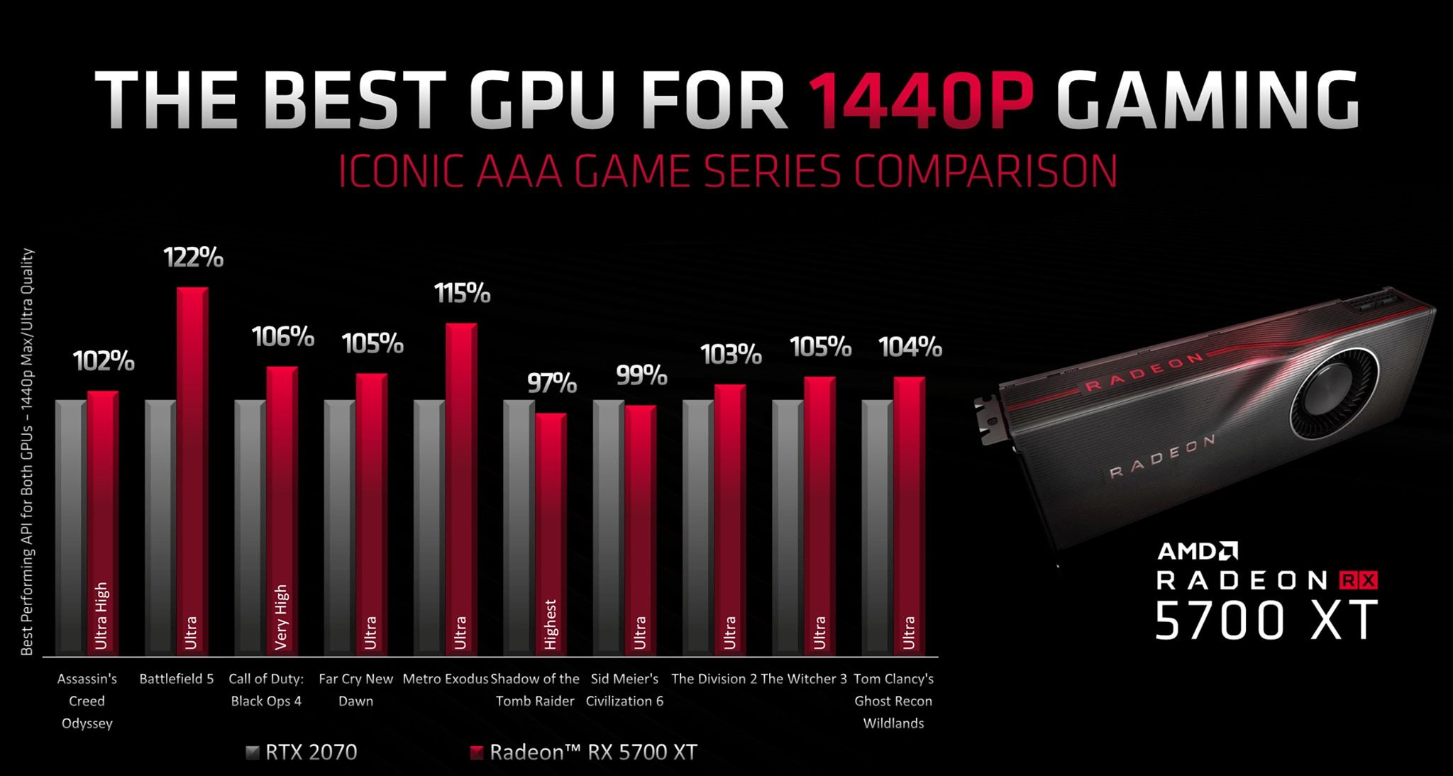
I think there is going to be some fallout if the RX 5700 and 5700 XT cards aren't performing as well in non-RT gaming benchmarks when compared to the RTX 2070/2080 cards. And a real shitstorm if they're lagging behind Vega 64 and/or R7 in benchmarks.

I find it quite telling that AMD is willing to show lots of benchmarks for their upcoming Ryzen 3000 series of CPUs beating Intel flagship processors in many benchmarks... yet, the only thing we got was an unclassified Navi product running Strange Brigade (which already favors AMD's prior architectures) for a product that's launching in week or so.
 
Last edited:
I think there is going to be some fallout if the RX 5700 and 5700 XT cards aren't performing as well in non-RT gaming benchmarks when compared to the RTX 2070/2080 cards. And a real shitstorm if they're lagging behind Vega 64 and/or R7 in benchmarks.

I find it quite telling that AMD is willing to show lots of benchmarks for their upcoming Ryzen 3000 series of CPUs beating Intel flagship processors in many benchmarks... yet, the only thing we got was an unclassified Navi product running Strange Brigade (which already favors AMD's prior architectures) for a product that's launching in week or so.
https://www.techpowerup.com/256422/...s-geforce-rtx-2070-in-a-spectrum-of-games?amp

QGj7xcBb1KE3qZFP.jpg
 
Cross posting from the other thread:

DG1000FGF84HT-PS4.
DG1101SKF84HV-PS4.
DG1201SLF87HW-PS4 Pro.
DG1301SML87HY-PS4 Pro.
DG14__________ - ???.
DG15 _
__________ - ???.
2G16002CE8JA2_32/10/10_13E9 - Gonzalo
ZG16702AE8JB2_32/10/18_13F8 - Gonzalo engineering sample

13E9 = Ariel https://pci-ids.ucw.cz/read/PC/1022/13e9
13E9 = Navi 10 Lite according to ChipHell post before all leaks. https://www.chiphell.com/thread-1945910-1-1.html

DG3001FEG84HR - Durango
DG4010T3G87E1 - Arlene SoC ??? Not sure what this is.
DG4001FYG87IA - XB1 S
1G5211T8A87E9 - Scorpio

DG02SRTBP4MFA - Subor Z
 
Last edited:
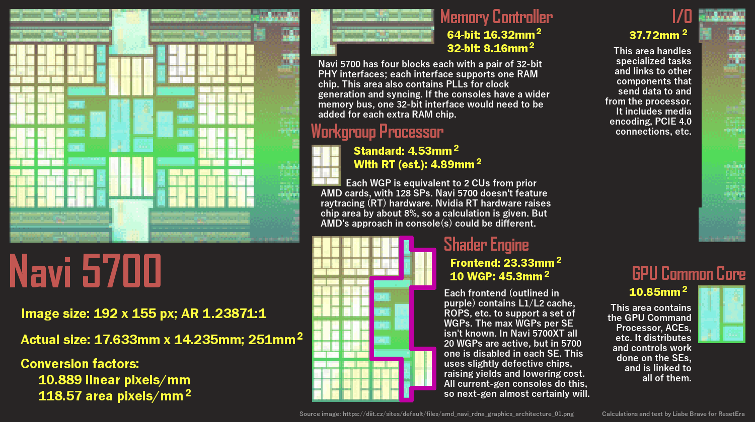
@Proelite would you mind doing a die size estimates breakdown for a possible next gen console APU with the following config:
32DCUs +10% added RT transistors, Zen 2, 320bit bus, 10 gddr6 memory controllers (20GB)
Same as point 1 but with 384 bit bus and 12 gddr6 memory controllers (24GB)

How much space would you estimate 64 rops and 256 tmu each take? Would a hypothetical 80CU card double the TMU-ROP count found in 5700 XT?
Would really appreciate a breakdown so i can scale up and down on my own

Zen 2 should be ~70mm2, might be smaller or larger based on how much of the L3 they decide to keep. Mostly likely smaller.

IO should be smaller on the consoles. Probably 20mm2.

Credit to Liara Brave of Resetera:

navibreakdownxuj6p.png
 
Last edited:
Zen 2 should be ~70mm2, might be smaller or larger based on how much of the L3 they decide to keep. Mostly likely smaller.

IO should be smaller on the consoles. Probably 20mm2.

navibreakdownxuj6p.png
THANK YOU!
A few questions if you don't mind
  1. Your previous estimates put the DCUs at 3.37 mm why the change to 4.53?
  2. Does 75mm for CPU in your previous estimate account for 32 mb cache?
  3. The GPU IO die can be shared with CPU or needs a separate one?
  4. Each SE contains 32 ROPs
  5. Read your previous posts on empty spaces found on 5700 are the accounted for in your estimates

1. i didn't include the supporting blank space silicon in the DCU, but filed them under the extra 140mm2.
2. yes
3. same
4. yes
5. nope. They were in the 140mm2. Liara Brave's picture that I linked does it correctly.
 
@boipucci

Your post on Era and Gaf used too much for the front end. You don't need 128 ROPS. Half that.
You can remove ~17mm2 from the IO as the console one won't have some stuff.

You're down to 391mm2. Which is within the realm of possibility.

7nm+ is not your savior. It's only a 10-15% die size reduction.
 
Your post on Era and Gaf used too much for the front end. You don't need 128 ROPS. Half that.
I used 4 SEs because i thought using only 2SEs would be a bottleneck (assumed 20CU per SE limit as seen on 5700xt)
Can you make the SEs smaller by halving the ROPs in each to 16? or just use 2SE?
7nm+ is not your savior. It's only a 10-15% die size reduction.
Thought 7nmEUV was 20%
6nm 15%

Thank you for the follow up, appreciate it.
 
I used 4 SEs because i thought using only 2SEs would be a bottleneck (assumed 20CU per SE limit as seen on 5700xt)
Can you make the SEs smaller by halving the ROPs in each to 16? or just use 2SE?

Thought 7nmEUV was 20%
6nm 15%

Thank you for the follow up, appreciate it.

If there is no 20CU per SE limit I would stick with 2SE, otherwise I would move to 3 for 60 CUs total. ~375mm2
Ur right 7nmEUV should be 15-20% according to TMSC, but I think 15% is the safe bet.
 
If there is no 20CU per SE limit I would stick with 2SE, otherwise I would move to 3 for 60 CUs total. ~375mm2
I see thanks, what's your take on redesigning the SEs (16ROPs each instead of 32) so that it takes less space (half) or wouldn't work?
 
I see thanks, what's your take on redesigning the SEs (16ROPs each instead of 32) so that it takes less space (half) or wouldn't work?
The number of ROPs would seem to be one of the reasons for the improved game performance of Navi. Reducing ROP capabilities would also be detrimental to providing good performance as the target resolution for the next gen consoles will be 4k (by whatever means, but still).
So it would be a design change that would be unfortunate for its target deployment.
If you want to reduce die area, you might be better off working with your lithographic process. Use TSMC 7nm+, use design rules that prioritizes density over clock speed (yielding a wider GPU at lower clock with a net small gain in perf/W at the cost of some die size vs. narrow design).
It may not make sense for a cost optimized PC part, but it may make sense for a console where power draw costs propagate throughout the final product.
 
Status
Not open for further replies.
Back
Top