Install the app
How to install the app on iOS
Follow along with the video below to see how to install our site as a web app on your home screen.
Note: This feature may not be available in some browsers.
You are using an out of date browser. It may not display this or other websites correctly.
You should upgrade or use an alternative browser.
You should upgrade or use an alternative browser.
Yes, but for the love of everything holy, they do not have any taste on colors they use.
Nope, you people dont get it. Performance and "quietness" is beautiful; when i see their color scheme in any PC pic, I instantly consider that PC prettier
It's not really new, you can find some RR numbers in the GFX databank since august 9th.
https://gfxbench.com/compare.jsp?benchmark=gfx40&did1=53156431&os1=Windows&api1=gl&hwtype1=iGPU&hwname1=AMD+Radeon(TM)+Vega+10+Mobile+Graphics&D2=Intel(R)+Core(TM)+i5-7260U+CPU+with+Iris(TM)+Plus+Graphics+640
https://gfxbench.com/device.jsp?D=AMD+Ryzen+5+2500U+with+Radeon+Vega+Graphics&testgroup=overall
>If you click on "Info", you will see:
OpenCL API | gfx901
OpenCL API | AMD Ryzen 5 2500U with Radeon Vega Graphics
gfx901 = APU's gpu part = 11 Compute Units
AMD Ryzen 5 2500U = CPU = 4C/8T = 8 CUs
So: both R5 2500U and R7 2700U will have 11 CUs! Cool!
https://gfxbench.com/compare.jsp?benchmark=gfx40&did1=53156431&os1=Windows&api1=gl&hwtype1=iGPU&hwname1=AMD+Radeon(TM)+Vega+10+Mobile+Graphics&D2=Intel(R)+Core(TM)+i5-7260U+CPU+with+Iris(TM)+Plus+Graphics+640
https://gfxbench.com/device.jsp?D=AMD+Ryzen+5+2500U+with+Radeon+Vega+Graphics&testgroup=overall
Not true.Videocardz said:https://videocardz.com/newz/amd-radeon-vega-8-and-vega-10-mobile-spotted
According to the listing at GFXBench it actually comes with 11 CUs, which means 704 Stream Processors. This number is quite odd, it’s also hard to understand why would Vega 8 have more cores than Vega 10, but well, this is all the information we have right now and it may not be accurate.
>If you click on "Info", you will see:
OpenCL API | gfx901
OpenCL API | AMD Ryzen 5 2500U with Radeon Vega Graphics
gfx901 = APU's gpu part = 11 Compute Units
AMD Ryzen 5 2500U = CPU = 4C/8T = 8 CUs
So: both R5 2500U and R7 2700U will have 11 CUs! Cool!
Last edited:
Actually I'm pretty sure they will have 8 and 10 CUs as suggested by the names. I suspect that current ESs have all enabled regardless of the final configuration, or some reporting issue or somethingIt's not really new, you can find some RR numbers in the GFX databank since august 9th.
https://gfxbench.com/compare.jsp?benchmark=gfx40&did1=53156431&os1=Windows&api1=gl&hwtype1=iGPU&hwname1=AMD+Radeon(TM)+Vega+10+Mobile+Graphics&D2=Intel(R)+Core(TM)+i5-7260U+CPU+with+Iris(TM)+Plus+Graphics+640
https://gfxbench.com/device.jsp?D=AMD+Ryzen+5+2500U+with+Radeon+Vega+Graphics&testgroup=overall
Not true.
>If you click on "Info", you will see:
OpenCL API | gfx901
OpenCL API | AMD Ryzen 5 2500U with Radeon Vega Graphics
gfx901 = APU's gpu part = 11 Compute Units
AMD Ryzen 5 2500U = CPU = 4C/8T = 8 CUs
So: both R5 2500U and R7 2700U will have 11 CUs! Cool!
D
Deleted member 13524
Guest
Actually I'm pretty sure they will have 8 and 10 CUs as suggested by the names.
Why?
I'm not even sure the max. number of enabled CUs is 11, since I only saw that number on leaked slides for embedded APUs.. Technically there are 12 NCUs in there..
Anarchist4000
Veteran
Presumably because of the model numbers. Vega 8/10/56/64. Being an APU, cutting an extra NCU for yields makes sense.Why?
I'm not even sure the max. number of enabled CUs is 11, since I only saw that number on leaked slides for embedded APUs.. Technically there are 12 NCUs in there..
Actually I'm pretty sure they will have 8 and 10 CUs as suggested by the names. I suspect that current ESs have all enabled regardless of the final configuration, or some reporting issue or something
Possible, but:
A10-9600P and A12-9700 have 6 CUs, but different GPU names: AMD Radeon™ R5 Graphics for A10-9600P and AMD Radeon™ R7 Graphics for A12-9700P (higher clocks).
FX™ 9800P, A12-9800B and A12-9720P have both 8 CUs and AMD Radeon™ R7 Graphics.
And about this ES: http://ranker.sisoftware.net/show_d...e8d9ff96ab8de5d8fe86bb9df89da090b6c5f8c0&l=en
Why?
I'm not even sure the max. number of enabled CUs is 11, since I only saw that number on leaked slides for embedded APUs.. Technically there are 12 NCUs in there..
There is a roadmap with upto 16 Compute Cores and 12 Next Gen GFX Cores, you're right, https://www.3dcenter.org/news/neue-roadmaps-praezisieren-amds-2017er-prozessoren-planungen
Somekind of FX Raven Ridge APU.
DUDE.Got the NH-U12s with the AM4 kit, looks quite nice
What DIMMs are those?
By the looks of them G.Skill TridentZ RGBs, just normal RGB coloring, don't know if there's any (3rd party or otherwise) app that would let you control them like thatDUDE.
What DIMMs are those?Lol, they look so yummy. Are the colors in any way influenced by memory accesses/activity, temperature or anything as such, or what?
DUDE.
What DIMMs are those?Lol, they look so yummy. Are the colors in any way influenced by memory accesses/activity, temperature or anything as such, or what?
Yup they are the G.SKill RGB ones, they look even better up close. You can change pretty much everything, you can even sync them with music playing on the PC.
I got them cheaper than the normal Trident Z ram so I can't complain
itsmydamnation
Veteran
tom hardware seems to have the best epyc hotchips coverage i have seen so far:
http://www.tomshardware.com/news/amd-threadripper-epyc-mcm-cost,35306.html
Not alot new, but there are quite a few slides on the Memory/cache/Io systems.
http://www.tomshardware.com/news/amd-threadripper-epyc-mcm-cost,35306.html
Not alot new, but there are quite a few slides on the Memory/cache/Io systems.
hoom
Veteran
http://techreport.com/news/32459/amd-ships-revised-ryzen-cpus-with-a-compile-bug-fix
Fixed hardware version for that previously discovered bug apparently.
Presume its just that later stepping thats used in Threadripper/Epyc -> AMD must have seen the bug & started to fix before Ryzen went live?
Fixed hardware version for that previously discovered bug apparently.
Presume its just that later stepping thats used in Threadripper/Epyc -> AMD must have seen the bug & started to fix before Ryzen went live?
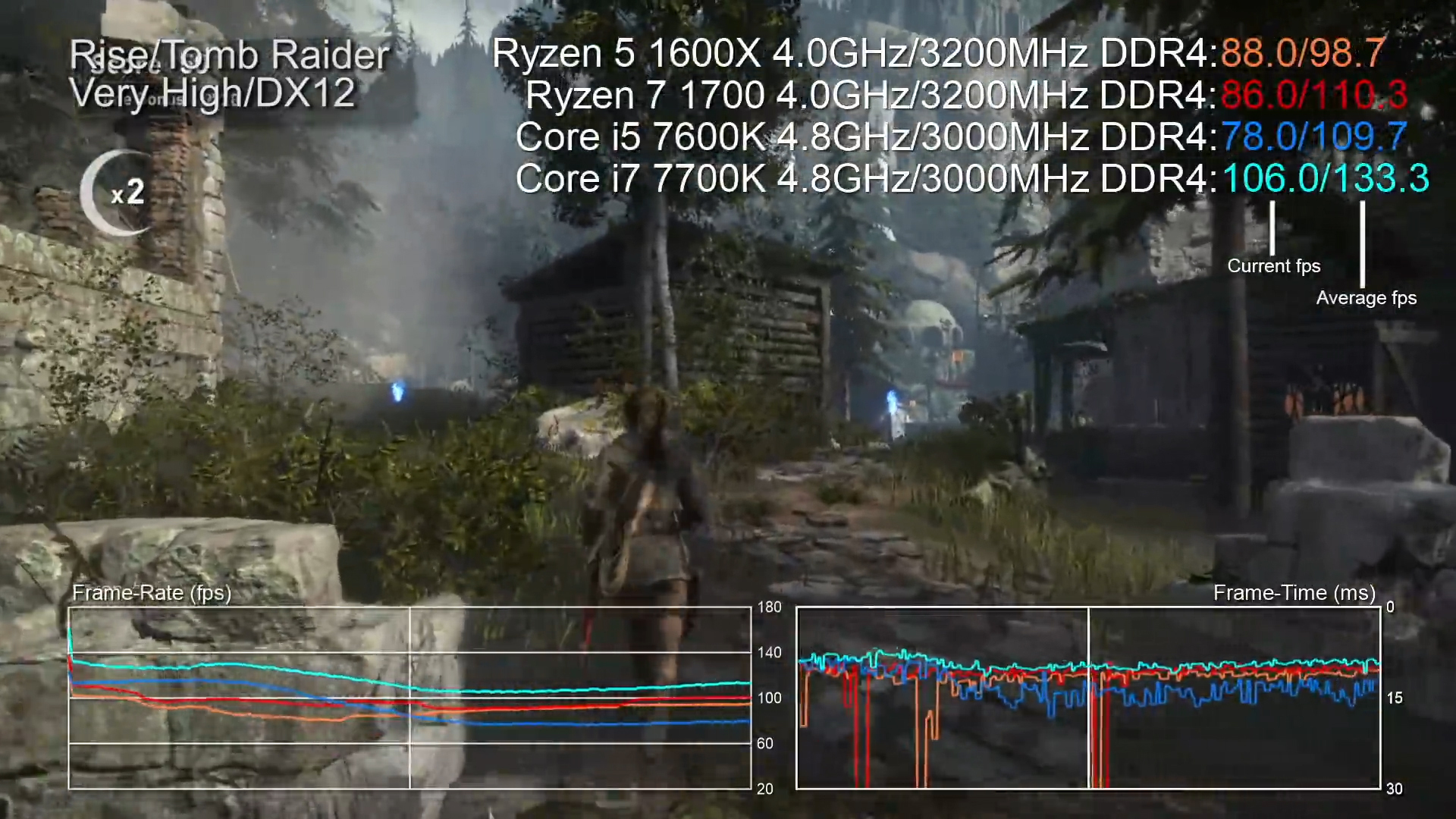
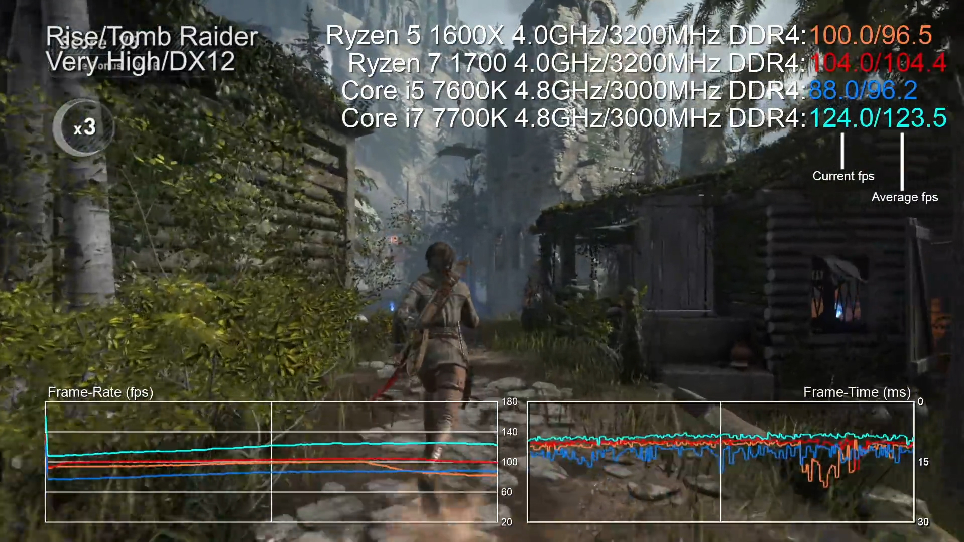
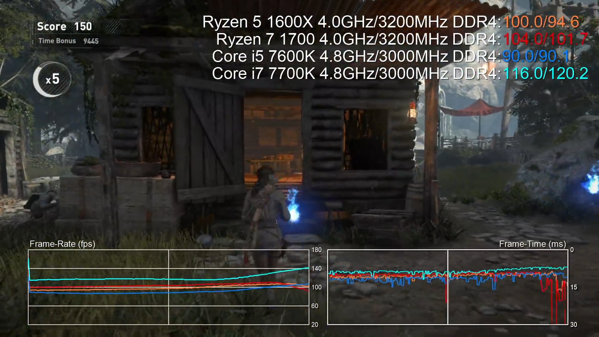
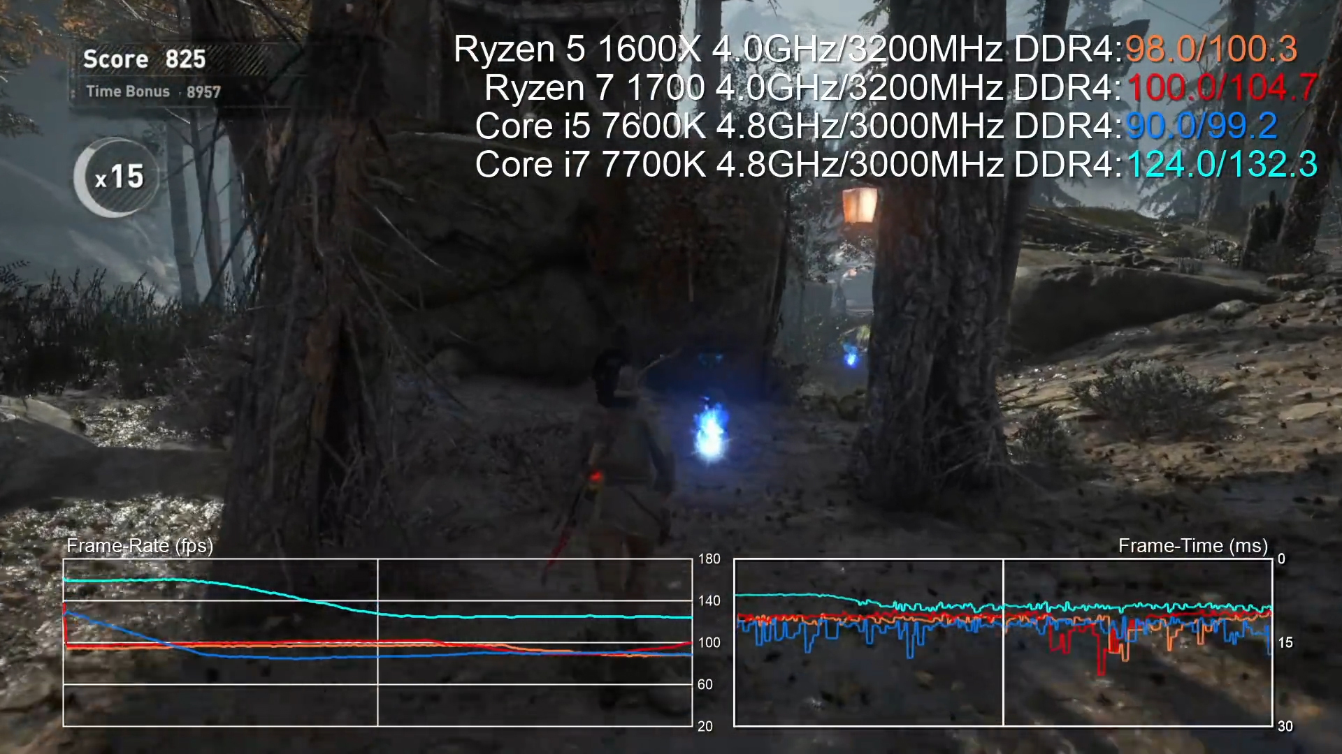
3200C14 with auto sub-timings vs 3466C14 with optimized sub-timings:
The bottom line is that both speed and sub-timings make a difference for Ryzen, the combination of both is ideal, not sure what the impact is for Intel platforms.
The bottom line is that both speed and sub-timings make a difference for Ryzen, the combination of both is ideal, not sure what the impact is for Intel platforms.
Last edited:
There's a slide that offers a bit more information on Zen's MDOESFI coherence protocol.tom hardware seems to have the best epyc hotchips coverage i have seen so far:
http://www.tomshardware.com/news/amd-threadripper-epyc-mcm-cost,35306.html
Not alot new, but there are quite a few slides on the Memory/cache/Io systems.
Above what was present in MOESI, the D state is defined as Dirty and listed as some kind of migratory sharing optimization.
It may be that F is Forwarding, like in MESIF, but it's not clear if that is the case.
That's taking AMD's protocol into a notably higher number of states than for its older architectures and Intel's, although short of the double digits of IBM's.
The slide doesn't quite get into what it takes for a line to go into the D or F state.
One possible interpretation is that AMD's protocol is trying to optimize the clean and dirty sharing paths. Under its MOESI protocol, there was some later wrinkles to the shared state, such as there being a little-discussed optimization for sharing where the requester got a shared line in the Owned state, and a potential state that was either in the caches or an intermediate directory/cache state that tried to optimize for sharing dirty lines that were to be modified shortly after (lock variables, etc).
Perhaps this has taken those optimizations and made them more formal. Another possibility, if AMD's choice is more like IBM's philosophy, there is information baked into these states about locality or probability of sharing.
Various reports indicate it doesn't need a new stepping, just a more recent production week like 25 or later.http://techreport.com/news/32459/amd-ships-revised-ryzen-cpus-with-a-compile-bug-fix
Fixed hardware version for that previously discovered bug apparently.
Presume its just that later stepping thats used in Threadripper/Epyc -> AMD must have seen the bug & started to fix before Ryzen went live?
That might mean there's some other way to make a small change on-die, or it's related to something besides the masks like new tests or changes in configuration or the packaging. Since this seems so inconsistent even among older chips, it might be discarding dies that were passing validation when they shouldn't. That may explain why the highly binned Threadripper is supposedly immune despite having B1 stepping just like Ryzen, although other elements like packaging and fuses may be different as well.
Similar threads
- Replies
- 61
- Views
- 11K
- Replies
- 90
- Views
- 17K
- Replies
- 220
- Views
- 92K


