Install the app
How to install the app on iOS
Follow along with the video below to see how to install our site as a web app on your home screen.
Note: This feature may not be available in some browsers.
You are using an out of date browser. It may not display this or other websites correctly.
You should upgrade or use an alternative browser.
You should upgrade or use an alternative browser.
AMD: R8xx Speculation
- Thread starter Shtal
- Start date
Jawed
Legend
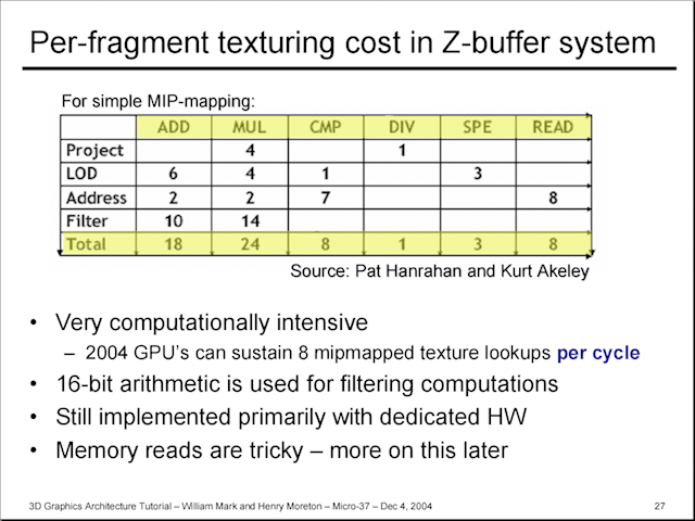
The addressing in NVidia's older GPUs ALUs is really just texture coordinate interpolation (calculation of the current pixel's texture coordinate, based on the 3 corners of the triangle and the texture coordinates at those 3 corners). Which the current GPUs also do in the multifunction interpolator ALU.Not much obviously -- NV40 and G70 series shared a whole ALU for it, but it's the sampling that is the dirty work, IMHO.

That's the "Project" part.
The TA part of NVidia's current GPUs is taking the coordinates, LOD and bias information to work out the address in RAM of a texel. That's the LOD and Address lines.
Jawed
Jawed
Legend
That may well be true.When you said that HD4770's performance is all the evidence we need that RV730's TUs were squandered.
I think that if RV740 had only 320 SPs but the same number of TUs, then it would ony lose 5-10% of performance or so with AA/AF enabled.
My assertion is that RV730 with 4 clusters with 4:1 ALU:TEX, instead of 8 clusters 2:1, would perform the same. But, not knowing the effect on most games of fp16 texture filtering (even at budget gamer settings?) I'm leaving a question mark over that conclusion.
In games with no fp16 filtering we can see this is probably true, because RV670 has exactly that configuration. HD3870 has more bandwidth and twice the colour rate of HD4670, though, but it does have the same Z rate. Generally HD3870 was slightly faster than HD4670 - don't know if things have changed.
Jawed
which tree/chip/plant/bush/card is this one?
Juniper XT ES, Water it weekly.
Meh, 4870/4890 performance w/ a 6pin at a (current) 4850 price...Meh -- drop one of the DVI ports and make room for all the hot air out.
Who wants that???
Edit- added the ()
Re-edit- Nice usage of the "original" RV740 cooler.
Jawed
Legend
http://www.guru3d.com/article/radeon-hd-4750-rv740-review-preview-test/3
The memory chip arrangement is very different. Did a 1GB HD4770 ever appear?
The power supply section of this board basically looks the same as HD4770.
Jawed
The memory chip arrangement is very different. Did a 1GB HD4770 ever appear?
The power supply section of this board basically looks the same as HD4770.
Jawed
http://www.guru3d.com/article/radeon-hd-4750-rv740-review-preview-test/3
The memory chip arrangement is very different. Did a 1GB HD4770 ever appear?
The power supply section of this board basically looks the same as HD4770.
Jawed
XFX released a 1GB 4770.
I can't find a 1GB HD4770. Neither the European nor US XFX sites have it.
Jawed
Ah yes, the links for 1GB parts all link to 512MB models.
http://www.wikio.co.uk/guide/xfx-radeon-hd-4770-1gb-206463.html
from 3dcenter ([fu]121Ah@work ):
8 memory chips on the front (can be seen on the old picture, or?) and 4 memory chips on the bag side (new picture) => 384bit ???
The one with 8 in the front was Cypress, the one with 4 in the back Juniper.
Jawed
Legend
What's going on with the top side of the heatsink retention clip? That side of the square is mostly "missing".
Jawed
Similar threads
- Replies
- 17
- Views
- 4K
- Replies
- 220
- Views
- 92K
- Replies
- 90
- Views
- 17K
- Replies
- 172
- Views
- 23K


