Two Antennas? Who Cares?
Here are the real questions!!! (Sorry Shift/Mods, Could Not Resist...)
Where Is Chipworks?!?
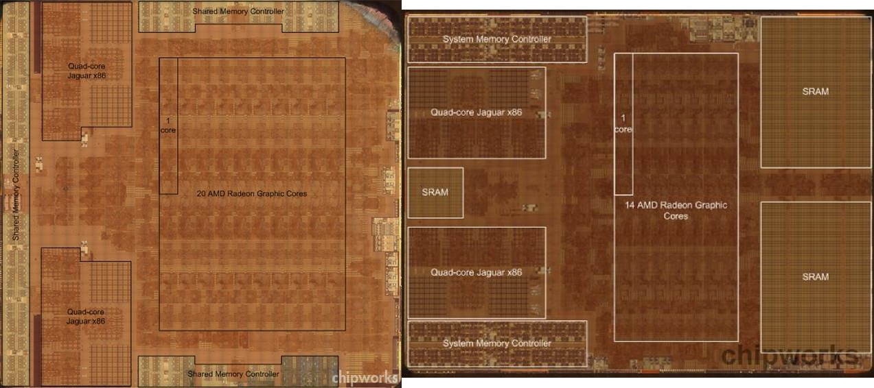
We want to compare the PS4 Jaguar images to the Xbox One "Custom (AMD) Processor" and see what is added/changed.
We want to compare the HP to HPM process cross sections of the transistors.
We want to see the Xbox One CU image next to the PS4 CU. The same CU? Added stuff? Native DP or just SP/CGN?
How about that eSRAM? 8T? 6T? Which 6T? Performance? Low Power? What??? 1T??? Then what the #$%^ else makes up the rest of the 5 BILLION transistors?
Any extra hardware directly connect to the eSRAM?
Anyone else want to see an Xray of a stacked die/3D/TVS design? [What?!? Is he joking? Serious? Sarcasm?!?]
Where is Chipworks? Kanata? Nepean? Maybe downtown? Gone over to Ottawa-Hull...? At the local bar? WHERE ARE THE XBOX ONE SoC IMAGES? On vacation today?
If I still lived there I would drive over and ask what the #$%^ are you people doing? (Likely drinking at this time on Friday. I guess Chipworks forgot to PRE-ORDER!!!! Or maybe their Xbox One actually works and they don't want to sacrifice it while their PS4 was DOA (Just kidding, not serious, please calm down. JUST A JOKE.))
Because matching VGLEAKS would be far too boring. And if they match VGLEAKS they must fire all of SIARCH immediately.
[I wonder what I am going to be dinged for this time?]
Last edited by a moderator:


