Predict: The Next Generation Console Tech

Status
Not open for further replies.
Or that MS' customisations to the existing AMD designs mean that it's a much more complex APU than AMD has produced thus far.

Yeah, if you think about it, it really sounds like a complex design:

1 APU (allegedly) contains:

8 x86 core
1 ARM core for security
1 DSP
GPU
Any other mystery block
Embedded Memory that's not a cache

Those things have to talk to each other and the outside world in some sort of fashion. Seems to me that it would be a really big challenge to get all those things working together efficiently.
 
I stumbled upon this slide from the Fusion Developer Summit which took place in June 2012. The slide deals with GPGPU algorithms in video games. There are a couple of details that are probably somewhat interesting when speculating about a next generation gaming console.

Thanks for posting that, I hadn't seen it before. You summarized it well.

I think some people were wondering why anyone would go with APU + GPU when you could just do an APU with a bigger GPU inside it. AMD sees it as a way to minimize latency and execution of GPGPU stuff on busy GPU's.
 
DDR3/4 1600 (a fairly moderate speed) would provide 102.4 GB/s on a 512bit bus if I'm not mistaken. So it would need a 1024bit bus to get near 192 GB/s but even then it would amount to 204.8 GB/s.

To get 192 GB/s you would need 1500Mhz memory on a 1024 bit bus. That sounds like a strange combination to me. Obviously 6Ghz GDDR5 on a 256 bit bus is a well known setup already being what the GeForce 670/680 use.

Could it be slower timed RAM to close timing in a high heat 2.5D environment?
 
I am not sure what is the best way for Sony when it comes to DDR4 and GDDR5 - both have their drawbacks especially if the desired bandwidth rumours are true. My main question is what is Sony taking so long since the current rumours point to a rather conservative hardware design. Either Sony is really waiting to cut cost or AMD/Sony engineers decided that something (HSA, stacking, HD8xxx, etc.) is worth the wait.
 
DDR3/4 1600 (a fairly moderate speed) would provide 102.4 GB/s on a 512bit bus if I'm not mistaken. So it would need a 1024bit bus to get near 192 GB/s but even then it would amount to 204.8 GB/s.

To get 192 GB/s you would need 1500Mhz memory on a 1024 bit bus. That sounds like a strange combination to me. Obviously 6Ghz GDDR5 on a 256 bit bus is a well known setup already being what the GeForce 670/680 use.

It could just be that the devkits have 192GB/s in a 6GHz 4GB GDDR5 config on a 256bit bus. Whereas the final silicon could have stacked DDR3/4 at 1600MHz on a 1024bit bus.

So rather the 192GB/s bandwidth is the devkit spec. and Sony has told devs that it would be either that or slightly above (i.e. 204.8GB/s).
 
And what does any of this have to do with gddr5 being hot and expensive? I'd say baseless.

Everybody knows that GDDR5 is hot&power hungry and expensive.. I was talking about the other part of his post -> I think that they using a 256bit memory controller and not an interposer.
 
Yeah, if you think about it, it really sounds like a complex design:

1 APU (allegedly) contains:

8 x86 core
1 ARM core for security
1 DSP
GPU
Any other mystery block
Embedded Memory that's not a cache

Those things have to talk to each other and the outside world in some sort of fashion. Seems to me that it would be a really big challenge to get all those things working together efficiently.


personally, call me crazy but i'm not expecting either next gen console to actually be an apu. rather, discrete cpu and gpu as usual.

it might make more sense for ms, as theoretically the jag cores may not take up that much die area anyway...
 
I am not sure what is the best way for Sony when it comes to DDR4 and GDDR5 - both have their drawbacks especially if the desired bandwidth rumours are true. My main question is what is Sony taking so long since the current rumours point to a rather conservative hardware design. Either Sony is really waiting to cut cost or AMD/Sony engineers decided that something (HSA, stacking, HD8xxx, etc.) is worth the wait.

Could simply be that they're waiting on the games being ready. Sony won't want a repeat of the PS3 where people had to wait 12 months for any worthwhile software. So they're waiting may have little to do with the HW design or manufacturing.
 
It could just be that the devkits have 192GB/s in a 6GHz 4GB GDDR5 config on a 256bit bus. Whereas the final silicon could have stacked DDR3/4 at 1600MHz on a 1024bit bus.

So rather the 192GB/s bandwidth is the devkit spec. and Sony has told devs that it would be either that or slightly above (i.e. 204.8GB/s).
Wouldn't that require a custom memory?
AFAIK, the stacking of DDR3/4 is the same width no matter how many layers in the stack, so it would need the memory to be like 32 chips on the interposer.
 
personally, call me crazy but i'm not expecting either next gen console to actually be an apu. rather, discrete cpu and gpu as usual.

it might make more sense for ms, as theoretically the jag cores may not take up that much die area anyway...

Why having 2+ dies when they are small? You gain something on yields but you loose over:
- latency and bandwidth between the 2 dies
- more complex motherboard design
- bigger packaging
- more complex cooling solution
Everybody in the industry is going toward SoCs. I think it will be a SoC.
 
Just for fun:

"Romance in Durango by Bob Dylan"

Maybe that's where the codename come from ;)

Anyway, the mistery sauce of Microsoft must be really great, because we haven't heard developers screaming about the lack of power of Durango..

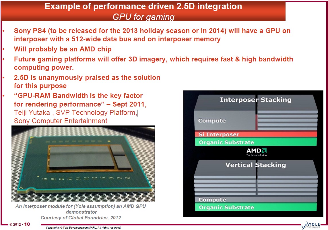
Rangers, you said there are 3 "external" custom hardware parts that can help the GPU. One is the audio DSP i guess, the other being some sort of fast cache coherent between the two (the SRAM).. the third one.. well it may be the most interesting one. Did we dismiss the interposer for good? The SoCs seems small, it could fit nicely on a interposer. Having hundreds of GB/s of bandwidth would surely impress the developers, making up for the lower raw power.

One of the blocks (the GPU one) could have something to do with textures supposedly?

That's really just mostly rumor though, nothing else.

Given what ERP said about texture reads being a problem with the slow main/fast ESRAM setup. it would make sense to have some sort of texture read special sauce, maybe...
 
Wouldn't that require a custom memory?
AFAIK, the stacking of DDR3/4 is the same width no matter how many layers in the stack, so it would need the memory to be like 32 chips on the interposer.

2 seperate 512bit stacks? the 2.5D pics we have seen seem to show a config like this. 8 x 2Gbit or 4 x 4Gbit layers each for 4GB.

95dd2b6d.jpg
 
Last edited by a moderator:
DDR3/4 1600 (a fairly moderate speed) would provide 102.4 GB/s on a 512bit bus if I'm not mistaken. So it would need a 1024bit bus to get near 192 GB/s but even then it would amount to 204.8 GB/s.

To get 192 GB/s you would need 1500Mhz memory on a 1024 bit bus. That sounds like a strange combination to me. Obviously 6Ghz GDDR5 on a 256 bit bus is a well known setup already being what the GeForce 670/680 use.

Could be, I'm going from vague memory on that one.
 
The 192 GB/s was some straight and easy 256 bus GDDR5 config IIRC.

Just as the 1.84 TF (very specific number) works out to exactly 1152 SP's at some clock or other, which was also the rumored SP/CU count. I remember BG Assassin pointing it out as a proof of it's veracity, that all the rumored specs fit each other perfectly.
 
Yeah, if you think about it, it really sounds like a complex design:

1 APU (allegedly) contains:

8 x86 core
1 ARM core for security
1 DSP
GPU
Any other mystery block
Embedded Memory that's not a cache

Those things have to talk to each other and the outside world in some sort of fashion. Seems to me that it would be a really big challenge to get all those things working together efficiently.

A challenge, yes but AMD now has experience doing this and it's even quite becoming the norm. Intel does APUs under the name of a CPU (with Quicksync as well as kind of a DSP), IBM does CPUs with a lot of coprocessors and edram, cell phone CPUs are basically like this as well.

Your objection can be done about current high performance GPUs alone. How can they work at all? :)
 
Everybody knows that GDDR5 is hot&power hungry and expensive.. I was talking about the other part of his post -> I think that they using a 256bit memory controller and not an interposer.
By what metrics are you using to base these conclusions on? Early days, when initially introduced, there was obviously clear delta's relative DDR3, but as the processes have moved on and the technologies and devices have evolved. From a heat / power perspective, for instance, take a look at the new notebook products announced; notebook segmentation is pretty much defined by available component TDP, and you can see that GDDR5 or DDR3 options are available on the same SKU. Power differences are very much in-line with the clock rates you run the things to achieve the data rates, but even if you bias down the voltage/clock of the core to compensate for the additional memory PHY power required for these datarates to stick within the same TDP you still end up with far great performance because the total memory power contributer is much lower than everthing else and the greater than doubling the datarate is far more useful.
 
The 192 GB/s was some straight and easy 256 bus GDDR5 config IIRC.

Just as the 1.84 TF (very specific number) works out to exactly 1152 SP's at some clock or other, which was also the rumored SP/CU count. I remember BG Assassin pointing it out as a proof of it's veracity, that all the rumored specs fit each other perfectly.

Would make sense for an early dev kit, get as close to target spec as possible with standard PC parts. I suspect they wont get final silicon in the dev kits until maybe 6 months before release.
 
The 192 GB/s was some straight and easy 256 bus GDDR5 config IIRC.

Just as the 1.84 TF (very specific number) works out to exactly 1152 SP's at some clock or other, which was also the rumored SP/CU count. I remember BG Assassin pointing it out as a proof of it's veracity, that all the rumored specs fit each other perfectly.

Which could just mean it was intelligently created. The actual veracity comes from the correct codenames in the pastebin dump, no?

Would make sense for an early dev kit, get as close to target spec as possible with standard PC parts. I suspect they wont get final silicon in the dev kits until maybe 6 months before release.

Which is only 4 months away.
 
Status
Not open for further replies.
Back
Top