Samsung Electronics plans to supply essential components for graphics processing units (GPUs), the high-bandwidth memory (HBM), and advanced packaging services to U.S.-based semiconductor company Nvidia.
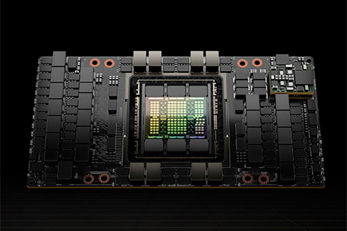
According to semiconductor industry sources on Aug. 1, Samsung Electronics is currently working with Nvidia on technical verification tasks for the HBM3 for GPUs and advanced packaging services. As soon as the technical verification procedures are completed, Samsung will supply HBM3 to Nvidia and is expected to take charge of the advanced packaging that processes individual GPU chips and HBM3 into a high-performance GPU, the H100.
Previously, Nvidia entrusted most of its GPU advanced packaging volumes to TSMC. TSMC produced Nvidia’s H100 by packaging SK hynix’s HBM3 on individual GPU chips manufactured through its own process. However, with the rapid increase in H100 demand due to the recent spread of generative artificial intelligence, TSMC struggled to handle all of Nvidia’s orders. Major clients such as Microsoft have announced service disruptions due to GPU shortages, prompting Nvidia to turn to Samsung Electronics, which has the capacity for both HBM3 and advanced packaging.
Currently, TSMC, a foundry company, is leading the advanced packaging race in the HBM and GPU sectors. The company has developed the “CoWoS,” a 2.5D package, over five generations for ten years from 2011 to 2021.
Samsung Electronics has also rolled up its sleeves to nurture advanced packaging. It unveiled a 2.5D packaging technology called “X-Cube” in 2021 and established an Advanced Packaging (AVP) team at the end of last year. It is known that starting from the second quarter of next year, the company will mass-produce the “X-Cube4,” which places four HBMs with the GPU, and “X-Cube8,” which places eight HBMs, in the third quarter. Samsung is expected to supply Nvidia with the third-generation HBM, or HBM3, by the end of this year and to use X-Cube4 to package it with individual GPU chips.


