Install the app
How to install the app on iOS
Follow along with the video below to see how to install our site as a web app on your home screen.
Note: This feature may not be available in some browsers.
You are using an out of date browser. It may not display this or other websites correctly.
You should upgrade or use an alternative browser.
You should upgrade or use an alternative browser.
- Status
- Not open for further replies.
DavidGraham
Veteran
Tesla and Elon Musk are back buying NVIDIA GPUs in very large numbers. To the point that Elon is stating if NVIDIA would supply them with enough GPUs, Tesla wouldn't think about building a Dojo Supercomputer.

 finance.yahoo.com
“We’re using a lot of Nvidia hardware,” Musk said during the earnings call. “We’ll actually take Nvidia hardware as fast as Nvidia will deliver it to us. Tremendous respect for [CEO] Jensen [Huang] and Nvidia. They’ve done an incredible job.”
“If [Nvidia] could deliver us enough GPUs, we might not need Dojo, but they can’t,” Musk said.
Tesla CEO Elon Musk: 'We're using a lot of Nvidia hardware'
Tesla CEO Elon Musk says the company is using a large amount of Nvidia hardware to power its AI tools.
D
Deleted member 2197
Guest

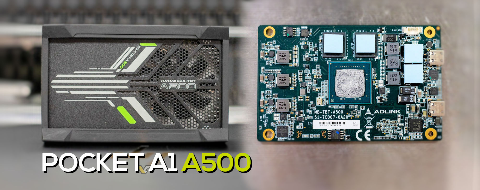
Adlink Pocket A1 portable 25W NVIDIA RTX A500 GPU is at least twice as powerful as Intel iGPU - VideoCardz.com
A GPU not bigger than a deck of playing cards ADLINK had an idea to launch a small and portable GPU that could be used at any time. ADLINK Pocket AI GPU, Source: StorageReview What is hidden inside is a NVIDIA RTX A500 GPU with 4GB of RAM. It is an external GPU that is […]
...
However, for those developers and researchers on the move with a lightweight laptop featuring only Intel graphics, an alternative in the form of this pocket GPU solution might give them the boost they require.
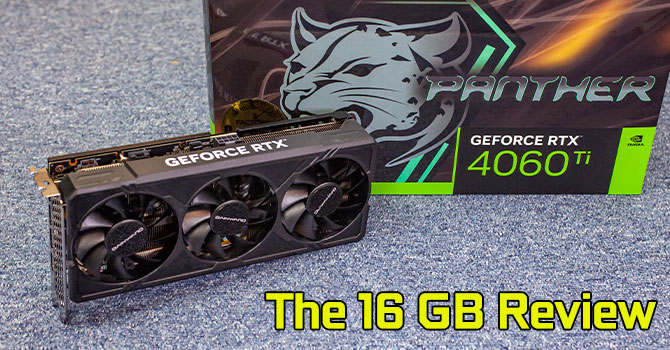
TechPowerUp's review of the RTX 4060 Ti 16GB is out. As expected (by many, at least), there is hardly any benefit for this level of card to have 16GB outside of heavy raytracing at 4k (or content creation, which this review does not test). Outside of Doom Eternal, Far Cry 6, and Resident Evil 4, the games tested at those settings don't show much difference and some aren't even playable. Naturally, this card (from Gainward) uses more power in all test scenarios.
 www.techpowerup.com

NVIDIA GeForce RTX 4060 Ti 16 GB Review - Twice the VRAM Making a Difference?
Finally! Our GeForce RTX 4060 Ti 16 GB review is live. We're investigating what performance gains you can expect from doubling the VRAM size to 16 GB. Our review of the 16 GB version also looks at power consumption and how overclocking is affected by the additional four memory chips on the back...
D
Deleted member 2197
Guest
Nvidia Launches AI Factories in DGX Cloud Amid the GPU Squeeze
Nvidia is now renting out its homegrown AI supercomputers with its newest GPUs in the cloud for those keen to access its hardware and software packages.
The DGX Cloud service will include its high-performance AI hardware, including the H100 and A100 GPUs, which are currently in short supply. Users will be able to rent the systems through Nvidia’s own cloud infrastructure or Oracle’s cloud service.
...
Tesla CEO Elon Musk last week talked about shortages of Nvidia GPUs for its existing AI hardware, and that Tesla was waiting for supplies. Users can lock down access to Nvidia’s hardware and software on DGX Cloud, but at a hefty premium.
The DGX Cloud rentals include access to Nvidia’s cloud computers, each with H100 or A100 GPUs and 640GB of GPU memory, on which companies can run AI applications. Nvidia’s goal is to run its AI infrastructure like a factory — feed in data as raw material, and the output is usable information that companies can put to work. Customers do not have to worry about the software and hardware in the middle.
The pricing for DGX cloud starts at $36,999 per instance for a month.
That is about double the price of Microsoft Azure’s ND96asr instance with eight Nvidia A100 GPUs, 96 CPU cores, and 900GB of RAM, which costs $19,854 per month. Nvidia’s base price includes AI Enterprise software, which provides access to large language models and tools to develop AI applications.
The rentals include a software interface called the Base Command Platform so companies to manage and monitor DGX Cloud training workloads. The Oracle Cloud has clusters of up to 512 Nvidia GPUs with a 200 gigabits-per-second RDMA network, and includes support for multiple file systems such as Lustre.
All major cloud providers have their own deployments of Nvidia’s H100 and A100 GPUs, which are different from DGX Cloud.
Google earlier this year announced the A3 supercomputer with 26,000 Nvidia H100 Hopper GPUs, which has a setup that resembles Nvidia’s DGX Superpod, which spans 127 DGX nodes, each equipped with eight H100 GPUs. Amazon’s AWS EC2 UltraClusters with P5 instances will be based on the H100.
With lock down, also comes lock-in — Nvidia is trying to get customers to use its proprietary AI hardware and software technologies based on its CUDA programming models. It could provide costly for companies in the long run, as they would pay for software licenses and GPU time. Nvidia said investments in AI will benefit companies in the form of long-term operational savings.
The AI community is pushing open-source models and railing against proprietary models and tools, but Nvidia has a stranglehold on the AI hardware market. Nvidia is one of the few companies that can provide hardware and software stacks and services that make practical implementations of machine learning possible.

kopite7kimi on Twitter: "I'm afraid there won't be RTX 4090 Ti anymor…
archived 27 Jul 2023 16:05:38 UTC

kopite7kimi on Twitter: "Combined with multiple sources, I confirm th…
archived 27 Jul 2023 16:05:54 UTC
If you have no competition at the ultra high-end in gaming, and you're probably selling all the better yielding AD102 dies as RTX 6000 cards for $6,800 (at least according to this comparison between the 4090 and RTX 6000 at Tom's), I suppose it makes no sense to release a 4090 Ti.
With respect to the 512-bit memory interface on the Ada-next flagship, I suppose that means one or more of the following: (1) GDDR7 won't be ready, and the next card would be bandwidth starved by a 384-bit bus using GDDR6x; (2) Nvidia now thinks it'll be cheaper to use a 512-bit bus instead of a massive hunk of SRAM as cache, greatly expanding die size, to get the effective bandwidth the card needs; (3) Nvidia is concerned that AMD will challenge at the high-end next generation and wants to push its own flagship as far as possible; (4) Ada-next (or at least the flagship) uses a chiplet approach that scales to 512-bit (not sure this last one makes technical sense). I'm sure I'm missing other obvious reasons.
With respect to the 512-bit memory interface on the Ada-next flagship, I suppose that means one or more of the following: (1) GDDR7 won't be ready, and the next card would be bandwidth starved by a 384-bit bus using GDDR6x; (2) Nvidia now thinks it'll be cheaper to use a 512-bit bus instead of a massive hunk of SRAM as cache, greatly expanding die size, to get the effective bandwidth the card needs; (3) Nvidia is concerned that AMD will challenge at the high-end next generation and wants to push its own flagship as far as possible; (4) Ada-next (or at least the flagship) uses a chiplet approach that scales to 512-bit (not sure this last one makes technical sense). I'm sure I'm missing other obvious reasons.
DegustatoR
Legend
People seem to think that G7 will launch at peak speeds proposed in the spec.
It is far more likely that G7 will launch just a tad higher than where G6X is right now.
So the need for a wider bus makes sense.
As for on-die cache it is likely a one time trick and they've done it with Ada already.
Plus SRAM don't scale below N5 so you can't increase the cache much - unless you're willing to try the N31/32 route.
With respect to the 512-bit memory interface on the Ada-next flagship, I suppose that means one or more of the following: (1) GDDR7 won't be ready, and the next card would be bandwidth starved by a 384-bit bus using GDDR6x; (2) Nvidia now thinks it'll be cheaper to use a 512-bit bus instead of a massive hunk of SRAM as cache, greatly expanding die size, to get the effective bandwidth the card needs; (3) Nvidia is concerned that AMD will challenge at the high-end next generation and wants to push its own flagship as far as possible; (4) Ada-next (or at least the flagship) uses a chiplet approach that scales to 512-bit (not sure this last one makes technical sense). I'm sure I'm missing other obvious reasons.
(5) The rumour is nonsense.
(5) The rumour is nonsense.
Ha, that could be the case. But, Kopite has a well-established track record of leaks, probably the best as far as Nvidia leakers go in the recent years. So, unlike leaks from many other leakers, this one has a place in forum speculation in my book.
As mentioned above, cache doesn't scale at all with N3 vs N5 so increasing cache is not a performance boost anymore (ie because you sacrifice ALU for cache on the die). Higher VRAM bandwidth is the way to go moving forward (of course with the usual software tricks that Nvidia is used to introduce in every generation aka DLSS3 and so on). I also want to point out that HBM is not out of the equation for next gen top SKU with the availability next year of high density HBM modules. Think about it, only 2 HBM modules will be needed to reach 2TB/s and 32GB with price somewhat "competitive" with 16 GDDR7 dies and a bigger / more complex PCB...If you have no competition at the ultra high-end in gaming, and you're probably selling all the better yielding AD102 dies as RTX 6000 cards for $6,800 (at least according to this comparison between the 4090 and RTX 6000 at Tom's), I suppose it makes no sense to release a 4090 Ti.
With respect to the 512-bit memory interface on the Ada-next flagship, I suppose that means one or more of the following: (1) GDDR7 won't be ready, and the next card would be bandwidth starved by a 384-bit bus using GDDR6x; (2) Nvidia now thinks it'll be cheaper to use a 512-bit bus instead of a massive hunk of SRAM as cache, greatly expanding die size, to get the effective bandwidth the card needs; (3) Nvidia is concerned that AMD will challenge at the high-end next generation and wants to push its own flagship as far as possible; (4) Ada-next (or at least the flagship) uses a chiplet approach that scales to 512-bit (not sure this last one makes technical sense). I'm sure I'm missing other obvious reasons.
Regarding chiplets, top Ada-next SKU may be using it but still not engraved in stone, only in advanced design stage right now... Hope Jensen will give the green light as it will be the biggest performance uplift ever of gen over gen. But the company is all about AI right now so I highly doubt it
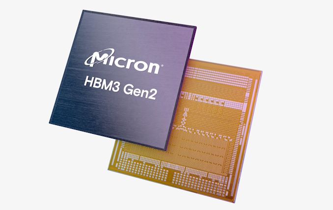
Edit: just see this new Anandtech article:
Last edited:
arandomguy
Veteran
From my understanding the actual direct cost of HBM is only a part of the overall cost issue. The other half is both testing for and dealing with defects compared to GDDR. The issue being that defect testing is much more costly/time consuming and that a significant portion of defects can slip through until basically final testing when everything is on package and those defects unlike with GDDR would essentially result in a loss of the entire package including the GPU die itself.
As for the 512 bit discussion the other angle here is that it might be a way to increase VRAM targeting segments other than consumer gaming. The economics might support targeting the segment below the highest HMB chip (eg. x00) with perhaps x02 shifting further towards that segment.
As for the 512 bit discussion the other angle here is that it might be a way to increase VRAM targeting segments other than consumer gaming. The economics might support targeting the segment below the highest HMB chip (eg. x00) with perhaps x02 shifting further towards that segment.
Decent enough progress, but GDDR development has been going just as well, if not better. So it's probably been something of a stalemate in terms of cost and performance considerations for consumer parts. HBM continues to offer more bandwidth potential compared to a GDDR alternative, but always at a notably higher price. It's just an inherently more expensive setup.Has there been so little progress with HBM that a 512 bit bus is preferable? It has been almost 10 years since Fury X and 8 since Vega 64.
Last edited:
Stacking opportunities exist now. CDNA3 is using L3/Infinity Cache chips underneath the core chips. This grants a lot of scope to further increase cache sizes without bloating overall die size. It's still a lot of total silicon, but we know better yields with smaller dies can beat one monstrous die in terms of cost. Plus because SRAM isn't scaling with process anymore, you can continue to use an older process for such cache chips.As mentioned above, cache doesn't scale at all with N3 vs N5 so increasing cache is not a performance boost anymore (ie because you sacrifice ALU for cache on the die).
Last edited:
TopSpoiler
Regular
Nvidia H100 GPUs: Supply and Demand
This post is an exploration of the supply and demand of GPUs, particularly Nvidia H100s.
One thing to note about the 512-bit bus and GDDR7 is that with 24Gb modules means you can have a 48GB on one side. Since there's rumours of Titan Ada coming again I can see Nvidia doing like a 48GB AD102 with two sides of the PCB being used and then a Blackwell Titan using just one side with 24Gb modules ala 3090 > 4090. And if GB100 is 512-bit bus monolithic die I can see the following used for that die:
- GB100 Quadro 96GB (best yields).
- Blackwell RTX Titan 48GB (second best yields).
- GeForce Now 5090/5090 Ti (anything that cannot make it as the previous two gets turned into this ala AD102 defective dies get turned into GeForce Now 4080s rather than using AD103 dies).
DegustatoR
Legend
GB100 is presumably a successor to GH100.
Thus a successor to AD102 would be GB102.
I also very much doubt that we will see a new Titan card any time soon. The point of these were to promote GPU compute and GPU ML by providing the h/w for that at a cheaper price than what you'd have to pay for similar Tesla/Quadro options. And that is something which hardly needs a promotion at the moment.
- Status
- Not open for further replies.
Similar threads
- Replies
- 84
- Views
- 7K
- Replies
- 375
- Views
- 32K
- Locked
- Replies
- 260
- Views
- 25K

