AMD: Speculation, Rumors, and Discussion (Archive)

Status
Not open for further replies.
Well the Q4 P100 PCie version, ... no FP16 support, no Nvlink ( only compatiblle with IBM chipset anyway ( outside GPU to GPU ). And i soomewhat can imagine that the most "available " one on Q4 will be the salvaged one. ( due to HBM2 ).

OK I can confirm the PCIe version does support mixed precision FP16 in same way as the Nvlink model, makes sense as they are both GP100.
Here is the spec for both:
Difference is clocks, power requirements, HBM2, along with NVLink.
Precision performance for the PCIe P100 model is 4.7/9.3/18.7
Table spec at bottom: http://www.nvidia.co.uk/object/tesla-p100-uk.html
The PCIe variant is meant to be priced around $5k to $5.5k, which is why it will (AMD has some breathing space with its timeframe of Q4) put pressure on the S9170 both from price/performance and top performance.
Will put less pressure on the S9300, but that depends upon the client requirements with regards to FP16, where the Fiji Pro card has same performance for FP32 and FP16 at theoretical 13.9 Tflops (ignoring application integration-optimisation).
Of course it also depends where the big Vega sits in all of this, more from the Pro-HPC-research perspective and AMD's strategy.

Cheers
 
Last edited:
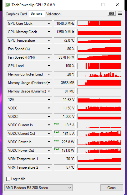
my 290 reports even more than that 480 (and wouldn't vddc power in more or less be card powerÅ=:
836.png
 
my 290 reports even more than that 480 (and wouldn't vddc power in more or less be card powerÅ=:

Add 30-50W from "GPU VRM Power In (PIN)" under "GPU [#1]: ATI/AMD Radeon R9 290: CHiL/IR PMBus - GPU Aux" in HWINFO, and that should be it.
"VDDC Power In" is GPU related power, while this accounts for mem related consumption.
At least that's how I'm doing it. It's probably wrong, but looks like a good approximation.
 
This thread reveals far more about forum posters than about the RX480.
You need to forgive certain posters, I think; 3D graphics/gaming enthusiasts tend to be very bored and disappointed with mid-range graphics cards. We're not really equipped to appreciate such hardware... :p
 
You're disappointed in a card that hasn't been released because it's apparently not competing with a card that doesn't even exist yet?

Was. But benchmarks were false, so no worrying at all.


You need to forgive certain posters, I think; 3D graphics/gaming enthusiasts tend to be very bored and disappointed with mid-range graphics cards. We're not really equipped to appreciate such hardware... :p

Power and area efficiency matters very much. And card is meant to compete with 16nm cards, competition will be tougher than it will be on day 29.

And btw i'm not the kind of guy who games at 4k, or buys $400+ graphics cards.

my 290 reports even more than that 480 (and wouldn't vddc power in more or less be card powerÅ=:
836.png

Wizzard from Techpowerup said the sensor only report the GPU power consumption, the rest of PCB power can't be estimated by its sensors.
 
Better geometry/discard + increased clocks will get there.
Given the lack of actual data, I'd like to hijack this comment for a quick education about better discard: what is it and what are the opportunities that are allegedly still open to be exploited?

I'm assuming the better discard is geometry based? What is possible other than backface removal?

Or they talking about better pixel discard? And, if so, is there a lot of thing to be improved there?
http://gpuopen.com/geometryfx-1-2-cluster-culling/
 
You need to forgive certain posters, I think; 3D graphics/gaming enthusiasts tend to be very bored and disappointed with mid-range graphics cards. We're not really equipped to appreciate such hardware... :p
:smile2:
Fair enough.
I think AMD had slightly too long between reveal and reviews, and that they missed an opportunity to for instance have an architectural presentation a couple of weeks after the reveal, when initial reactions had quieted down and everyone interested was hungry for more. They could have presented their story and get full attention, but without performance numbers to maintain interest at its peak for reviews.
Oh well, only four days to go now. Tech sites will get hammered.
 
http://twvideo01.ubm-us.net/o1/vault/gdc2016/Presentations/Juha_Sjoholm_DX12_Explicit_Multi_GPU.pdf


http://gpuopen.com/wp-content/uploa...ogramming_Model_and_Hardware_Capabilities.pdf

Here you can find some summary tables about typical VR memory costs per frame: http://alex.vlachos.com/graphics/Alex_Vlachos_Advanced_VR_Rendering_Performance_GDC2016.pdf

With some simple maths you can see, just only for frames buffers, how easily prohibitive can VR, HDR and 4K with in a high frame-rate scenario become...
And still NVIDIA seems to be confident their 2GB/s is enough on the new SLI HB bridges
You forgot to mention that in the very next slide they say they can actually hide around 15ms worth of latency from copying, and that the "limits to 60 fps" is just in case of one specific multiGPU rendering method, which is useful for AFR with temporal effects.
In case of VR, they don't use AFR to begin with, but each GPU (assuming 2 GPUs present) handle one eye
 
:smile2:
Fair enough.
I think AMD had slightly too long between reveal and reviews, and that they missed an opportunity to for instance have an architectural presentation a couple of weeks after the reveal, when initial reactions had quieted down and everyone interested was hungry for more. They could have presented their story and get full attention, but without performance numbers to maintain interest at its peak for reviews.
Oh well, only four days to go now. Tech sites will get hammered.
Even though I think AMD marketing department needs a serious clear. I think this is part of their strategy, as good or bad as it may be, and they committed to it.

Creating hype is very dangerous. If the product don't show of in the reveal then it will backfire and destroy the product. We will have to wait a couple of days only.

Enviado desde mi HTC One mediante Tapatalk
 
In my experience GPU-Z VDDC Power In matches quite nicely with what I measure at wall minus the system. And that's 250W peak benching Firestrike on a 290.

But at the end of the day GPU-Z just displays what sensors report.
 
Last edited:
That's a software technique. Does it require any special hardware?

Sorry, i should have explain, this was for replace the lacking of efficiency on culling in hardware on previous generation, this shoud give an idea on what have aim GCn4.0 in hardware. but it will indicate that they can basicay cull everything now, even by cluster.. The technique described there + mbcnt fast compaction http://gpuopen.com/fast-compaction-with-mbcnt/ is just working amazingly well on old generation. ( why this have not been implemented on benchmark and game before ? ) .

Im pretty sure, given the timeline, that GCN4.0 is solving much of it directly in hardware instead of the need to rely to special software path.

Im prettty sure that if someone take the OpenGL tesselation test and add this line code, we could seen surprising result.
 
Last edited:
It would AFAIR be unprecedented if AMD allowed voltage adjustment from their own control panel. Then again, it's not like they don't know the limitations of the chip, so why not give a little margin to play around with.

Then you don't know the AMD CPU overclocking tool Overdrive.
 
Sorry, i should have explain, this was for replace the lacking of efficiency on culling in hardware on previous generation, this shoud give an idea on what have aim GCn4.0 in hardware. but it will indicate that they can basicay cull everything now, even by cluster...
It still doesn't seem like a technique that's generally applicable to existing workloads. The kind that will make them decisively win benchmarks today...

(If anyone of the AMD web team is reading this: your site is pretty much unusable on iOS with both safari and chrome...)
 
The hype is still way over the top for a midrange card.

I don't know why there should be less hype for a midrange card. What I think is hype-worthy is how efficient a design is, how much performance it can squeeze out of each watt, each mm², each GB/s. Whether the RX 480 really deserves this hype, well, we'll know on the 29th.
 
Speculating on this one, but DCC for a framebuffer copy would probably speed things along. ATW might also avoid the issue as you would warp the old frame. As for the links, I thought they were primarily handling signaling with actual data transfers occurring over PCIE.

HPC versions of Vega could be interesting with that high speed link. While Nvidia is limited to IBM processors, AMD could add the link to a HPC focused Zen. That should be the only x86 option with a high bandwidth interconnect. I'm sure there are some applications with memory bottlenecks out there that could use that.
 
And still NVIDIA seems to be confident their 2GB/s is enough on the new SLI HB bridges
You forgot to mention that in the very next slide they say they can actually hide around 15ms worth of latency from copying, and that the "limits to 60 fps" is just in case of one specific multi-GPU rendering method, which is useful for AFR with temporal effects.
In case of VR, they don't use AFR to begin with, but each GPU (assuming 2 GPUs present) handle one eye
NVIDIA always say a lot of things.... It's called marketing.
It's not about AFR. Its about frame buffering transferring and resource coupling. Limit bandwidth impact both and both are engaged in every multi-GPU techniques. Yes, there are some tricks, like MSAA upscaling, but those tricks are not a real solution.
Bandwidth is one the biggest issue on today's computing.
 
Status
Not open for further replies.
Back
Top