AMD: RDNA 3 Speculation, Rumours and Discussion

Status
Not open for further replies.
You're now getting to my point. We have some nebulous "Ampere is x times faster than Turing for ray tracing". You reference two games, Dying Light 2 and Control and instead of using the data points for Ampere versus Turing to validate whether those games and their RT performance are even worth discussing, you just ignore the possibility of validating your technique.

Actually I'm struggling to understand your point. I don't care what Nvidia marketing claimed. I'm using actual measured performance in real games. What do you mean by "validate whether those games and their RT performance is worth discussing"? What is your criteria for validation?

In the same way we can validate whether TFLOPS is a useful metric for determining gaming performance, we could validate whether the claim about RT speed-up is useful.

NVidia has made claims about RT speed-up with Ampere. We could use game performance to validate those claims. We might find games that align with those claims.

I have no idea whether it's possible to validate those claims of RT speed-up. With respect to RDNA 3 you've proposed a technique, but not tested it.

You misunderstand. I am not interpreting the 2x and 3.5x rumours as AMD's marketing claims of performance improvement. I am using them as measured performance in a game with RT off (2x) and on (3.5x) and scaling up 6900xt numbers (again real measured performance) accordingly.
 
I tried to calculate effective bandwidth of Navi 31 based on the rumor about 4TB/s physical bandwidth of the Infinity Cache and extrapolated hit-rate for 4K resolution:

for 16 Gbps GDDR6 @384bit (768 GB/s):
  • 192MB IC: 3512 GB/s
  • 256MB IC: 3840 GB/s
  • 384MB IC: 3963 GB/s
for 18 Gbps GDDR6 @384bit (864 GB/s)
  • 192MB IC: 3608 GB/s
  • 256MB IC: 3936 GB/s
  • 384MB IC: 4059 GB/s
for 21 Gbps GDDR6 @384bit (1008 GB/s)
  • 192MB IC: 3752 GB/s
  • 256MB IC: 4080 GB/s
  • 384MB IC: 4203 GB/s
Given the info about enhanced bandwidth-saving techniques of RDNA 3 (more advanced implementation of delta-compression) it almost looks like an overkill. Navi 21 had 1664 GB/s effective bandwidth.
(It would be 3912-3976-4072 GB/s for the previously rumored combination of 512MB IC + 256bit 16-18-21 Gbps GDDR6 and 3584-3648-3744 GB/s for hypothetical combination of 256MB IC + 256bit 16-18-21 Gbps GDDR6.)

Maybe smaller IC + 384bit bus + slower GDDR6 is a more cost-effective combination regarding the TSMC's price hike(?)
 
What is your criteria for validation?
I'm asking the question, is your interpretation useful? I'm suggesting that you should determine the usefulness of your interpretation.

For example, you can make an interpretation about the performance impact of TFLOPS, when comparing 5700XT and 6700XT. Luckily, data for both is available, so you can qualify your interpretation.

My criteria for validation are centred upon taking existing games with existing cards and seeing whether theoretical RT performance differences are a good predictor of actual performance. You might find that for some games the prediction is good. Or you might find that within a specific architecture the prediction is good, e.g. 6900XT versus 6600XT.

You misunderstand. I am not interpreting the 2x and 3.5x rumours as AMD's marketing claims of performance improvement. I am using them as measured performance in a game with RT off (2x) and on (3.5x) and scaling up 6900xt numbers (again real measured performance) accordingly.
The issue is that in some games the impact on AMD for RT is very large and in others much less. So, when does that 3.5x apply? We would hope it's not the latter!

Your motivation for choosing DL2 and Control may well be to pick the worst cases on RDNA2 with the expectation that they will benefit the most. I dunno, I can't read your mind.

I'm not saying you shouldn't make an interpretation. I'm trying to suggest that there's a chance you can improve the quality of the interpretation, or provide some caveats.

Being honest, 5.6x faster

7900xt = 37.1/6.6 = 5.6x faster than the 6900xt in pure RT. That would be amazeballs.
is pretty unbelievable :oops: It needs to be about 6x faster, yes, to be competitive with Ada, but it seems unlikely...
 
For example, you can make an interpretation about the performance impact of TFLOPS, when comparing 5700XT and 6700XT. Luckily, data for both is available, so you can qualify your interpretation.

My criteria for validation are centred upon taking existing games with existing cards and seeing whether theoretical RT performance differences are a good predictor of actual performance. You might find that for some games the prediction is good. Or you might find that within a specific architecture the prediction is good, e.g. 6900XT versus 6600XT.

Again, none of the numbers I’m using are theoretical or marketing. The flops analogy is incorrect. I’m only using actual measured performance for all my calcs. The only assumption I’ve made is that the leaked 2x and 3.5x numbers are measured performance.

The issue is that in some games the impact on AMD for RT is very large and in others much less. So, when does that 3.5x apply? We would hope it's not the latter!

It’s not mathematically possible for Navi 31 to be both 2x faster than the 6900xt without RT and 3.5x faster with RT in games with low RT usage. E.g. Far Cry 6. So yes the rumored performance increase has to be in “heavy” RT games.

Your motivation for choosing DL2 and Control may well be to pick the worst cases on RDNA2 with the expectation that they will benefit the most. I dunno, I can't read your mind.

Yes games with material RT usage have the most potential to demonstrate significant gains for Navi 31. See above.

Being honest, 5.6x faster is pretty unbelievable :oops: It needs to be about 6x faster, yes, to be competitive with Ada, but it seems unlikely...

Yes, I did say it would be amazeballs :) Im just running math based on the rumors not making any claims as to the validity of those rumors.
 
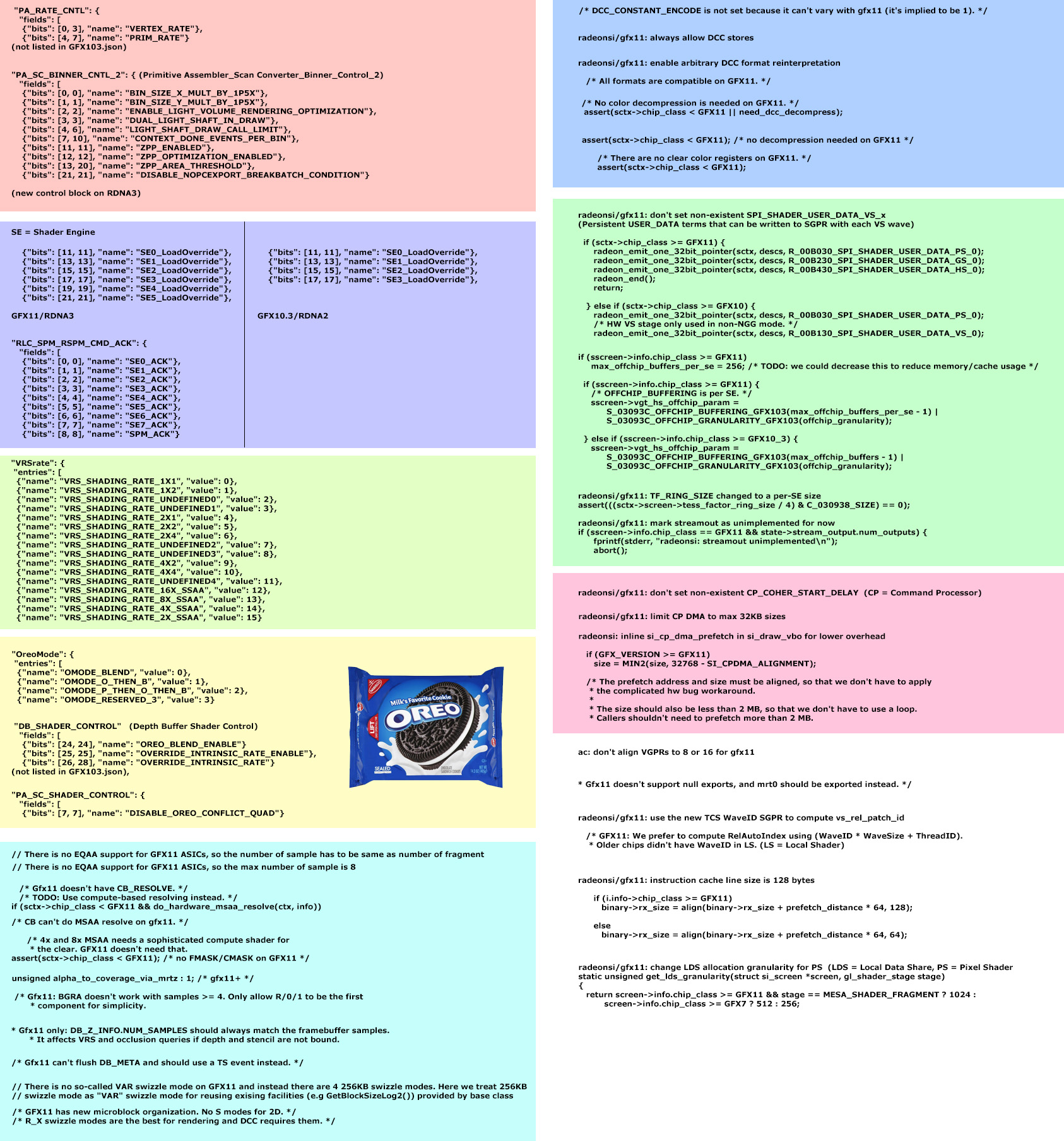
This image:

FR9rFSuWYAAsaPw


which comes from here:


summarises things quite nicely.

I notice the Oreo Mode relates to the Depth Buffer, but has "Blend" as an entry as well as two others with "O then B" and "P then O then B". I don't know what those letters mean. Perhaps:
  • O = overwrite
  • B = blend
but P I don't have a suggestion for. "Blend" doesn't apply as an operation to a depth buffer. It could either mean that the colour buffer is in blend mode, so depth should be untouched. Or perhaps these letters relate to the way MSAA samples are written. So blend would imply a read/modify/write.

P could mean "predicate" which implies a mask, I suppose. Or pixel?

I can't work out what P then O then B would amount to though - an implied sequence puzzles me.

Alternatively these could refer to sizes in a hierarchy: e.g. pixel size and then sample size? So the sequence might imply a set of scales at which testing/updating is performed.

Obviously an Oreo has depth and the two biscuits can be thought of as triangles and the filler as the new operation: as the way they are resolved against each other in a depth buffer operation (including MSAA samples).

Or, the other way around, the filler is a triangle and the biscuits refer to operations upon that, to determine front and back bounds for the operation.
I still don't have a resolution for the O, P, B symbols, but I think the answer to the "Oreo mode" question is hinted by:

⚙ D125824 [AMDGPU] gfx11 export instructions (llvm.org)

where we see "ET_DUAL_SRC_BLEND0" and "ET_DUAL_SRC_BLEND1", seemingly with the introduction of the dual source blending concept in the export of pixels.

This seems to explain it:

Dual-source blending in DirectX 11 — Roderick's Debug Diary (roderickkennedy.com)

I suppose that each of these operations (0 and 1) are implemented in sequence, and perhaps they can be assigned as any function, not just multiply and add as shown in that example.

Overall, honestly, I know pretty much nothing about dual source blending.

This doesn't help much:

Output-Merger Stage - Win32 apps | Microsoft Docs
 
Given the info about enhanced bandwidth-saving techniques of RDNA 3 (more advanced implementation of delta-compression) it almost looks like an overkill. Navi 21 had 1664 GB/s effective bandwidth.
(It would be 3912-3976-4072 GB/s for the previously rumored combination of 512MB IC + 256bit 16-18-21 Gbps GDDR6 and 3584-3648-3744 GB/s for hypothetical combination of 256MB IC + 256bit 16-18-21 Gbps GDDR6.)

Maybe smaller IC + 384bit bus + slower GDDR6 is a more cost-effective combination regarding the TSMC's price hike(?)
If they do make a massive cache like 384MB, it's probably to help with RT which would love more bandwidth. The RT cache requirements and hit rate is probably different than what AMD had on their RDNA2 cache slide.
 
Sigh, I've only just noticed that AMD refers to Wave64 mode instruction issue in RDNA as "dual-issue":

AMD PowerPoint- White Template (gpuopen.com)

see slide 17, "Wave64 via dual-issue".

So the comment "Dual-Issue Wave32 could mean at the same time and not one after another, as for Wave64?" from


now makes more sense to me. I'd totally missed the explicit use of the "dual-issue" term by AMD.

Also covered here:

Optimizing for the Radeon RDNA architecture (gpuopen.com)

with accompanying video:


Following the pattern from RDNA1/2, I'm going to guess that RDNA 3 uses SIMD16 VALUs and so a "large" VOPD instruction issues to the SIMD on alternating cycles, perhaps suggesting that the hardware thread size in RDNA 3 is 16, not 32. So, two consecutive instructions from a shader are coded into a VOPD, which provides a saving on instruction read rate (but maybe not on instruction cache size).

This would then imply that the entire instruction set is coded as VOPD, with VOP1/2/3 being exceptions in cases of serial instruction dependency.

That's a pretty massive conceptual change. Which makes it kinda unlikely. But then, erm, RDNA was a pretty massive conceptual change over GCN...
 
[snip]

That's a pretty massive conceptual change. Which makes it kinda unlikely. But then, erm, RDNA was a pretty massive conceptual change over GCN...

A few circumstanial counter arguments:

1. RDNA's goal is to reduce the # of wavefronts needing to keep the hardware busy. Requiring VLIW2 bundles for full rate issue is a regression — code sequences not being able to meaningfully produce a long VLIW2 run will get only 1 VALU issue per 2 cycles, and in turn requires 2x wavefronts to fully light up the pipelines. This is also assuming that the CU front-end can pack 2 instructions from 2 different wavefronts as well, in absence of any VLIW2 bundle ready to be issued.

2. Wave64 has not required a "dual-issue" instruction encoding to begin with. It is a hardware execution mode that accepts the same instructions as Wave32, and VGPR indexes being transparently taken care of in operand collection. If they do reduce the SIMD hardware width to 16 lanes, what would be the benefits to complicate the ISA and the SIMT model this time around? Why not having Wave16 as the native mode, and implementing Wave32 like today's Wave64 over 32 lanes?

3. That usage of "dual-issue" in the talk feels more of a one-off outlier, since the mainstream understanding of "dual-issue" generally implies co-issuing. The RDNA 2 ISA manual itself does not describe Wave64 as "dual-issue" as well, but rather "issuing the instruction twice".
 
So far, there is no "flavour" beyond wave32 and wave64:


so that shoots down my theory of wave16, while wave64 still seems to be part of RDNA3:


A few circumstanial counter arguments:

1. RDNA's goal is to reduce the # of wavefronts needing to keep the hardware busy. Requiring VLIW2 bundles for full rate issue is a regression — code sequences not being able to meaningfully produce a long VLIW2 run will get only 1 VALU issue per 2 cycles, and in turn requires 2x wavefronts to fully light up the pipelines. This is also assuming that the CU front-end can pack 2 instructions from 2 different wavefronts as well, in absence of any VLIW2 bundle ready to be issued.
Agreed to all that, except I'm very sceptical that the hardware will do on the fly VLIW2 bundling.

VLIW2 might only be for 16-bit operands, which now seem to be first class citizens of RDNA 3 (vector registers and LDS). So the full-rate issue problem might not be introduced for normal instructions with 32-bit operands, only for instructions with 16-bit operands that use VOPD. At least shaders containing those instructions will have lower register pressure (when counted in terms of 32-bit register size).

With Super SIMD, specifically Do$, sequential instruction dependency problems are reduced, presumably there'll be less than 5 clocks of latency in that case.

2. Wave64 has not required a "dual-issue" instruction encoding to begin with. It is a hardware execution mode that accepts the same instructions as Wave32, and VGPR indexes being transparently taken care of in operand collection. If they do reduce the SIMD hardware width to 16 lanes, what would be the benefits to complicate the ISA and the SIMT model this time around? Why not having Wave16 as the native mode, and implementing Wave32 like today's Wave64 over 32 lanes?
So far, there's no indication in code of wave16 (I think we should assume it's not coming), but that doesn't eliminate SIMD-16.

3. That usage of "dual-issue" in the talk feels more of a one-off outlier, since the mainstream understanding of "dual-issue" generally implies co-issuing. The RDNA 2 ISA manual itself does not describe Wave64 as "dual-issue" as well, but rather "issuing the instruction twice".
Yes, this use of "dual-issue" insults my senses.

By the way, looking at slides 9 and 10:


it appears that GCN could not do transcendental instruction issue in parallel with the VALU, and worse, these instructions could not even overlap.

In RDNA it looks like transcendental instruction issue takes the place of VALU issue, so there is still only one vector instruction issue per clock, but at least they can overlap.

So, that simplifies the vector register read and write porting and bandwidth questions we had earlier.
 
One plausible case for 16-lane SIMD IMO is that:

(1) The native wavefront size remains 32 lanes, including the VRFs, operand collectors and the memory pipelines (which seem to happily remain 128-byte cache lines);

(2) Two 16-lane SIMDs as the VALU pipelines. Native 32-wide wavefronts are executed on them with double issuing and transparent half skipping like Wave64.

(3) Compiler scheduled co-issuing (VOPD) is introduced to offset the potential ILP lost caused by double issuing. Probably no change to instruction latencies, except for cross-lane modifiers/instructions that will have to deal with partial bypass hazard (note: `S_DELAY_ALU`?).

(4) VALU issue rate: up to 2 VALU instructions (from two different waves) or 1 VOPD bundle per cycle; the 2 inst/cycle rate can only be sustained with either VOPD or having >=1 half-disabled Wave32 in flight.

This way they will not regress on achievable ILP on paper (still 1.0). Meanwhile, it can potentially execute some divergent kernels better, provided that these kernels will either naturally converge to one half of the wavefront, or will explicitly reorder the lanes at sync points e.g. a wave ballot+shuffle.

This also doesn't pose much questions on the VRF and memory pipelines, since they can remain 32-lane wide. Though a possible crack in this theory would be whether/how the VRF can sustain 2x half-disabled wave32s being co-issued at full rate for long VALU runs. :?:
 
Last edited:
I will take some time to digest your post. In the meantime I can suggest another possibility, since reading your post prompted it.

A dual-configuration SIMD: SIMD32 for 32-bit resultants OR SIMD64 for 16-bit resultants, which uses VOPD to issue a pair of instructions to use the doubled lanes.

[EDIT: this is a stupid post because it's not saying anything new - I've been alluding to VOPD for 16-bit resultants for ages, so this just expresses that in another way, and is pointless.]
 
Last edited:
One plausible case for 16-lane SIMD IMO is that:

(1) The native wavefront size remains 32 lanes, including the VRFs, operand collectors and the memory pipelines (which seem to happily remain 128-byte cache lines);

(2) Two 16-lane SIMDs as the VALU pipelines. Native 32-wide wavefronts are executed on them with double issuing and transparent half skipping like Wave64.

(3) Compiler scheduled co-issuing (VOPD) is introduced to offset the potential ILP lost caused by double issuing.
I know you said "two 16-lane SIMDs" (and in that case instruction throughput would be halved), but I think it would be four per CU. This is based upon my theory that VOPD for 32-bit resultants is not happening. The risk of not being able to use VOPD is too high due to serial dependencies (eating-up more hardware threads), whereas for 16-bit resultants the cost of serial dependencies preventing use of VOPD is relatively low, because relatively little code has 16-bit resultants.

(FWIW, I think deleting the RBEs in favour of shader code is a great use of VOPD for 16-bit resultants. Most render targets are 8- or 16-bit per component).

Incidentally, I think four SIMD16 per CU, with two CUs per WGP means that two GCDs each of 48 WGPs are required for Navi 31/32.

Probably no change to instruction latencies, except for cross-lane modifiers/instructions that will have to deal with partial bypass hazard (note: `S_DELAY_ALU`?).
I thought I'd collect some new-due-to-GFX11 hazards:


Code:
  bool hasVALUPartialForwardingHazard() const {
    return getGeneration() >= GFX11;
  }

  bool hasVALUTransUseHazard() const { return getGeneration() >= GFX11; }
neither of those are being used yet.

Meanwhile these were added in a commit:

Code:
let SubtargetPredicate = isGFX11Plus in {
  def S_WAIT_EVENT : SOPP_Pseudo<"s_wait_event", (ins s16imm:$simm16),
                                 "$simm16">;
  def S_DELAY_ALU : SOPP_Pseudo<"s_delay_alu", (ins DELAY_FLAG:$simm16),
                                "$simm16">;
} // End SubtargetPredicate = isGFX11Plus

With DELAY_FLAG (GFX11) being printed like so:


Code:
    static const std::array<const char *, 12> InstIds = {
      "NO_DEP",        "VALU_DEP_1",    "VALU_DEP_2",
      "VALU_DEP_3",    "VALU_DEP_4",    "TRANS32_DEP_1",
      "TRANS32_DEP_2", "TRANS32_DEP_3", "FMA_ACCUM_CYCLE_1",
      "SALU_CYCLE_1",  "SALU_CYCLE_2",  "SALU_CYCLE_3"};
[...]
      static const std::array<const char *, 6> InstSkips = {
      "SAME", "NEXT", "SKIP_1", "SKIP_2", "SKIP_3", "SKIP_4"};

Is that telling us that there's four VALUs? Similarly, is that telling us that there's three transcendental ALUs? In my opinion, no for both of these. The compiler doesn't have a model of the relative number of ALUs (SALU, VALU, TRANS) because the compiler has a hardware-thread centric view, not a CU- or WGP-centric view.

Are the cycle counts for SALU telling us that SALU has a 3-cycle intrinsic loop?

I don't think S_DELAY_ALU is for intra-VALU timing hazards, instead it appears to relate to relationships amongst:

  • SALU and VALU or
  • SALU and TRANS or
  • VALU and TRANS
presumably for VCC validity or resultant availability. But, looking at:


we can see there's two categories of "delay" here, InstIds (which is for either a first instruction or a second instruction) and InstSkips which are just immediate skip counts. So the former case could, perhaps, be applied to intra-VALU timing hazards? Or is that for instructions with 16-bit resultants, used to work out when a "clause of VOPD" instructions can commence?

(4) VALU issue rate: up to 2 VALU instructions (from two different waves) or 1 VOPD bundle per cycle; the 2 inst/cycle rate can only be sustained with either VOPD or having >=1 half-disabled Wave32 in flight.
I strongly believe that the hardware cannot dynamically combine hardware threads for simultaneous issue in one cycle. The entire history of AMD GPUs shows no tendency towards instruction-issue that is outside of the compiler's direct control. If the compiler cannot see hardware threads, then the hardware cannot do simultaneous issue within a SIMD-type (either VALU or TRANS).

It seems to me that this S_DELAY_ALU instruction is specifically providing the compiler with the ability to control execution for a single hardware thread.

This way they will not regress on achievable ILP on paper (still 1.0). Meanwhile, it can potentially execute some divergent kernels better, provided that these kernels will either naturally converge to one half of the wavefront, or will explicitly reorder the lanes at sync points e.g. a wave ballot+shuffle.
I agree that SIMD16 is useful for half-hardware thread predication and also I agree that "wave ballot+shuffle" is an extremely attractive concept. The latter has been at the back of my mind in pretty much all RDNA 3 speculation, specifically because ray tracing puts enormous pressure upon work-item divergence.

This also doesn't pose much questions on the VRF and memory pipelines, since they can remain 32-lane wide. Though a possible crack in this theory would be whether/how the VRF can sustain 2x half-disabled wave32s being co-issued at full rate for long VALU runs. :?:
I think that's answered simply by VOPD being exclusively for 16-bit resultants :)

Anyway, overall, I think SIMD16 has a compelling feel to it, right now.
 

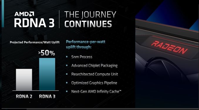
Official info from AMD in their Financial Analyst day

We're in for some nice performance gains, higher than before. Very impressive. Great times ahead in the pc space, good for competition as Intel/NV will try even harder.
Still huge leaps today due to architectural changes and added features and design choices. RX7600/7700 offering 6900XT performance atleast? If they double the infinity cache it'd be a native 4k monster aswell.
 
On first impressions it seems we're looking at two SIMD32s that share a single vector register file, which could then imply that there's only one SALU for each pair of SIMD32s. That would be a compute unit, I suppose and two compute units could make up a WGP, with the layout of L0, TMUs and RAs being the same as for RDNA 2.

I'm going to need to spend more time to understand the intricacies of register swizzling across the VRF banks. With VOPD in the mix, how does that all come together?...

What will be interesting to see is how small the VRF banks end up being, because the cache looks like it will be the sole source of operand reads for the pair of SIMDs, providing as much as 6 operands per clock.

Ideally, fingers-crossed, between L0, VRF and operand cache, the sizings mean that complex shaders no longer hit a performance wall due to high register allocation. In theory most registers will live outside of the VRF for these shaders and the access times and bandwidths will not limit SIMD throughput.

In the end registers tend to be "live" for only a very short section of a shader, so most registers in a complex shader will be written to only once or twice and then read only once or twice.

So a complex shader with, say, 76 registers allocated in the initial compilation, could end up being compiled with, say, 32 VGPRs, enabling many more hardware threads to be live. The bulk of the registers in this scenario live for a short time in the cache, being "evicted" once those registers have been read by the shader code for the final time.

Obviously, there are exceptions, e.g. a conventional matrix multiplication has a very high liveness (say 99%) and the live registers tend to cover 90%+ of the shader's length. But in that situation arithmetic intensity easily hides memory access latencies, so not many hardware threads are required to keep the SIMDs busy.

It may end up that the VGPR banks are the same size as seen in RDNA 2, but now those four banks feed two SIMDs, not one. So that would mean the effective quantity of memory assigned to VGPRs is halved.

Really this should be about making performance less brittle due to the quantity of registers allocated for complex shaders. But the compiler gets a lot more complicated, because it now needs to model the operand cache as well as the VRF. I wonder whether the cache can actually be fully modelled (allocations and timings) - in theory it can't because the compiler doesn't know what hardware threads are live in the CU. The compiler may be stuck with heuristics, inviting many years of compilation pain, trying to decide the maximum lifetime of a VGPR in cache or not using the cache and writing to VRF instead.

Alternatively, if the cache is extremely small, e.g. up to 3 operands per hardware thread per SIMD, then in theory the compiler's model is super simple and entirely predictable. Then it's a question of how many hardware threads are supported by the cache, e.g. is it 10 (some number that corresponds with the maximum count of hardware threads per CU) or just two, assigned as "lo" and "hi" dedicated to the live clause of either two hardware threads (wave32) or the upper and lower halves of a single hardware thread (wave 64). I suppose it could be some quantity of slots that is split equally across live hardware threads, but then the compiler has no model...
 
My quick gist is that this is nothing more than an elaboration of the previous super-SIMD patent, focusing on specifically the dual-instruction SIMD ALU pipeline:

- Each 32-lane SIMD unit now gets a second, likely symmetrical ALU pipeline.
- Operand cache/collector is expanded to sustain 6(+?) operands per clock, in order to support the second ALU pipeline.
(conveniently the patent did not say how they will serve operands to the (non-ALU) SIMD request/export buses...)
- VRF remains quad-banked (somewhat implied 1R1W banks), serving max. 4 operands per clock.
- The 6+ operands per clock rate can undoubtedly be sustained only if 2+ operands are served via bypass results from the VRF destination cache.
- Three ways of issuing 2 instructions per clock:
(i) issuing both halves of a Wave64 instruction in a single cycle; (paragraph 25)
(ii) one VOPD instruction, basically a single instruction with up to 6 operands (paragraph 32), presumably with potential of a pipeline stall when you use >4 operands;
(iii) two instructions, one each from two independent Wave32s. (paragraph 25)


It does not seem particularly groundbreaking change here (if we use changing hardware vector width as the ground). They are mostly trying to (dynamically?) exploit code sequences which rarely need to read a 3rd operand from the VRF, because either:
(i) they are dominated by 1-2 operand instructions; or
(ii) they often have long read-after-write chains where at least operands can frequently be served from the VRF destination cache, bypassing the VRF.
Such exploitation comes in the form of either ILP (one VOPD "dual instructions") or TLP (2 independent Wave32s or 1 Wave64).


Do note that both the operand "cache" and the result "buffer" as described in the patent are IMO existing architectural features, i.e., operand collection, and destination scheduling.


---

This is going to muddle the units for marketing a bit, pretty much like Ampere pretty much like how some people perceive Ampere's double FP32 support. On paper each CU does gain 2x the "Stream Processors", now having 128 SPs. Now depending on how AMD GPU marketing wants to draw the rectangles, it can either be "two dual-issue SIMD32s" or "four SIMD32s" inside each CU...
 
Last edited:
Status
Not open for further replies.
Back
Top