AMD: RDNA 3 Speculation, Rumours and Discussion

Status
Not open for further replies.
I'm not holding my breath for 7 chiplet solution, I think 2 G(raphics)C(compute)D(ies) + one IOD with all the cache (+ which could possibly be 4th die 3d stacked on top of the IOD) is more likely for first generation solution
So, sort of ironically, it almost doesn't matter how many chiplets there are, if there are chiplets. The die area (assuming 512MB of Infinity Cache) is going to be in that ball park.

Cache + GDDR PHY, alone, is in the region of 500mm². Whether in one 6nm chiplet or across several chiplets.

Obviously there is space taken by TSVs to join chiplets, but that's super dense. That's the whole point of hybrid bond, as seen in 5800X 3D, to provide massive bandwidth in a very small area.

It would be fun if AMD made a 600mm² base die on 6nm and then slapped two GCDs on top. So many ways to play with chiplet configurations!
 
How important/complicated is the SW aspect to a chiplet GPU relative to Crossfire/SLI AFR rendering on AMD’s end?

Should be largely dependent on what AMD is doing with the hardware. My current thought is that the leakers have the general specs right but not the hardware configurations. Most likely there's two 5nm GPU chiplets that can work by themselves or double up like the M1 Ultra can, and except for LLC all the other work dispatch and the ram PHYs and etc. are on each chiplet. Only one silicon bridge needed, only 1 chiplet by itself or 2 linked together max, keep complexity to a minimum. You cold easily get the leaked lineup with different bins of two chiplets. That's especially true of TSMCs more expensive packaging options versus Intel, who's plans rely on their heavy investment in good enough but reliable and relatively inexpensive packaging for putting all those different chiplets in.
 
Is there still cause for concern that erratic frametimes could be an issue a la microstutter?

Microstutter is due to different GPUs working on different frames with inconsistent frame pacing. That shouldn’t be a problem with multiple chiplets cooperating to render a single frame.
 
Microstutter is due to different GPUs working on different frames with inconsistent frame pacing. That shouldn’t be a problem with multiple chiplets cooperating to render a single frame.
If they are allowed to work on a single frame, that is. It was done on 3dfx' SLI, was touted as a possibility at both Nvidia-SLI and Crossfire launches and would have been an option for legacy MGPU. It just did not produce as much "avg. fps" gain as AFR.

Apparently, MI250(X) is seen as two independent devices from the drivers perspective. If that holds true for 1st gen gfx chiplet products, they could very well resort back to AFR again with a much faster chip-to-chip connection of course.

That would be shockingly disappointing and likely not possible. AFR under DX12 requires explicit game support.
 
That would be shockingly disappointing and likely not possible. AFR under DX12 requires explicit game support.
Yes, that's why it finally (and deservedly) died. But other than compute tasks, game graphics need some more communication between the chiplets, which either requires something thats in charge of decomposing the frame data and recomposing it at the end or (a lot of) driver overhead beforehand. It's more likely though, that something much more ingenious I'm not thinking of right now will solve this.

If you're willing to forego some of the flexibility, you could have dedicated area specific to some chiplets. I think 3DLabs tried this approach with dedicated chips (1×VSU+ 2×PSU) in their Realizm 800.
 
It's like all the patents reportedly linked to RDNA 3 describe the main desire for the MCM implementation be opaque to SW. Hopefully, these claims really do apply to RDNA 3 and not to a RDNA 3 + X.

// Found the recent patent describing a relatively straight-forward way to split pixel operations between chiplets:
...the GPU chiplet-based system includes GPU chiplets that are addressable as a single, monolithic GPU from software developer's perspective (e.g. the CPU and any associated applications/drivers are unaware of the chiplet architecture), and therefore avoids requiring any chiplet-specific considerations on the part of a programmer or developer.
 
Last edited:
The key to making a pair (or more) of compute chiplets work is in how geometry workloads and results are distributed, collated and re-despatched. Ideally temporary data (produced by vertex shaders or mesh shading) doesn't get pushed into VRAM, the worst case being a producer-consumer buffer that lives in L3 cache. That buffer needs to be fairly elastic, after all somewhere in the middle is tessellation.

Once rasterisation is started, then tiling takes over and all of the rendering is tile-based - this is already a feature of AMD GPUs. Sure there will be "global" buffers used in rendering, such as textures, shadow maps and bounding volume hierarchies, but those present mostly a global memory performance problem, which Infinity Cache directly attacks.

Compute algorithms that make heavy use of locality only have the option to implement locality at work item and work group levels, neither of which are affected by chiplets.
 
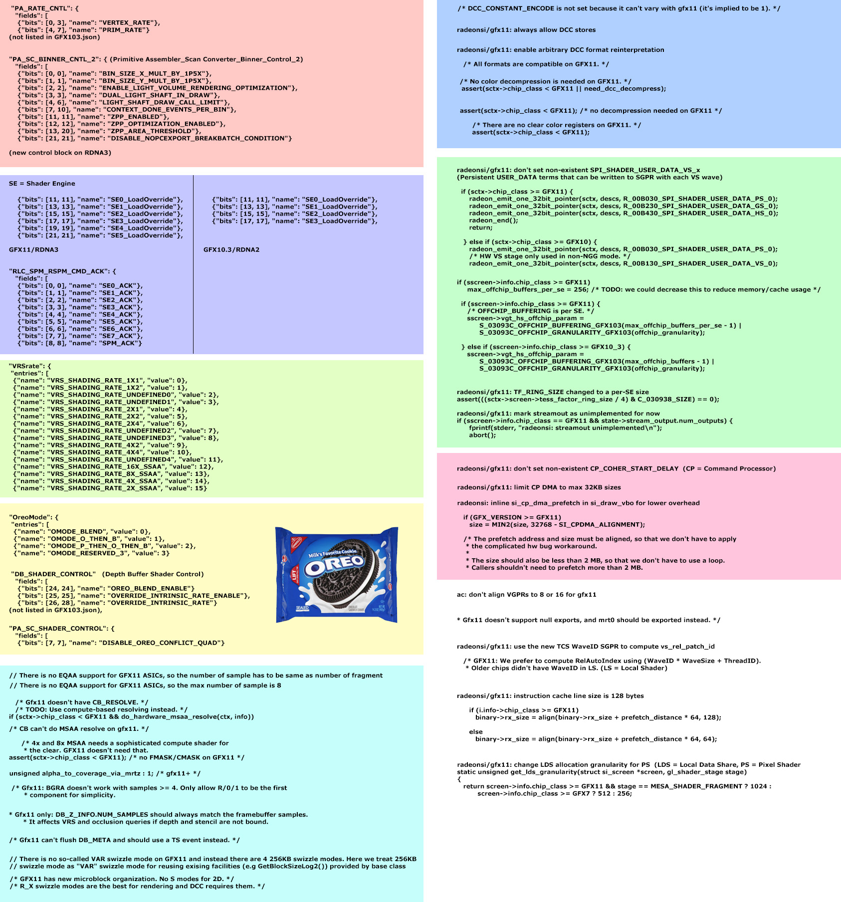
This image:

FR9rFSuWYAAsaPw


which comes from here:


summarises things quite nicely.

I notice the Oreo Mode relates to the Depth Buffer, but has "Blend" as an entry as well as two others with "O then B" and "P then O then B". I don't know what those letters mean. Perhaps:
  • O = overwrite
  • B = blend
but P I don't have a suggestion for. "Blend" doesn't apply as an operation to a depth buffer. It could either mean that the colour buffer is in blend mode, so depth should be untouched. Or perhaps these letters relate to the way MSAA samples are written. So blend would imply a read/modify/write.

P could mean "predicate" which implies a mask, I suppose. Or pixel?

I can't work out what P then O then B would amount to though - an implied sequence puzzles me.

Alternatively these could refer to sizes in a hierarchy: e.g. pixel size and then sample size? So the sequence might imply a set of scales at which testing/updating is performed.

Obviously an Oreo has depth and the two biscuits can be thought of as triangles and the filler as the new operation: as the way they are resolved against each other in a depth buffer operation (including MSAA samples).

Or, the other way around, the filler is a triangle and the biscuits refer to operations upon that, to determine front and back bounds for the operation.
 
https://github.com/llvm/llvm-projec...c64c4ffcdd456f2630288bbc523180772848713e9R692

Code:
def FeatureVOPD : SubtargetFeature<"vopd",
  "HasVOPDInsts",
  "true",
  "Has VOPD dual issue wave32 instructions"
>;

Static scheduling dual-issue, instead of twice the CU/SIMDs?
The implications for register file bandwidth/porting are significant.

Dual-issue would effectively, in the general case, require up to 6 input registers, e.g. FMA r3, r2, r1, r0 & FMA r7, r6, r5, r4. That's devastating for a register file!

Of course dual-issue instructions might not be offered in the general case (i.e. for all possible instructions). Instead there might be a very limited set of dual-issue instructions, e.g. purely for bitwise operations or for Int32 math.

I would like to see the removal of 3 operand VALU instructions, and instead they would be converted to a sequence of two instructions, with an intermediate result held within the VALU pipeline. I've been thinking about this for years, but its time may have come now.

A conventional series of instructions might look like:
Code:
FMA r3, r2, r1, r0
FMA r7, r6, r5, r4
ADD r8, r3, r7
SUB r9, r6, r2

but dual-issue with no more than 2 operands would look like:
Code:
MUL vi0, r1, r0 | MUL vi1, r5, r4
ADD r3, r2, vi0 | ADD r7, r6, vi1
ADD r8, r3, r7  | SUB r9, r6, r2

So this would still require the register file to support 4 operands, but at least that's not as disastrous as requiring 6.

Alternatively, dual-issue instructions might only support instructions where the pair only requires a total of 3 operands from the register file. So instead of using the register file bandwidth of 3 operands merely to support a single instruction that takes 3 operands, a subset of instructions is identified that's compatible with dual-issue where one of the pair has two operands and the other in the pair has one operand.

Or, where the two instructions share an operand.

There's still a problem with utilisation, due to instruction dependencies, which is something I'm very much not in favour of. But dependencies would be reduced a little if there were no 3 operand instructions.

Anyway, I doubt that this will be used as an alternative to doubling the count of VALUs. The way the rumour mill is going right now, though, it's clear that the mongers are doing 2 + 2 = 5 math, so their specifications are utterly useless.

When I do 2 + 2 = 5 math I am at the very least doing so in an explicitly speculative fashion :p
 
Was G80’s missing MUL ever found?
I can't remember.

I think multi-threaded issue became a factor in the speculation back then:

G80 programmable power | Beyond3D Forum

shame that the forum transition broke so many links (intra-forum as well as to images).

As for G80...
SYVaQOz.jpg

;)
I thought "missing MUL" was decided to be there, but only can be used with super specific type of case/program.
Which led to general "if you can't use it in 99% of the time - it's not in there" - type of thinking.

Maybe I should just open source these tests, and if someone still has both a G80 and a GT200 lying around in their basement they could give it a go ;) But then I'm a bit scared people would actually use them and take the results seriously on modern HW due to lack of alternatives, which wouldn't be a great idea...

agent_x007, where do these annotated die shots come from?! I've never seen that one from G80! You don't have an annotated die shot of NV30 by any chance? :p

---

And yes, Missing MUL was effectively not there (except for multiplying by 1/W for interpolation) but the really bizarre thing is how it evolved through both driver versions and hardware revisions. I swear that there was one driver revision on G80 where I actually had some of my old (lost to time) microbenchmarks use the MUL slightly more effectively, but then it reverted in later drivers to being practically never used. I really wish I wrote down that driver revision back then but now it's lost to time - maybe it was just buggy...

So I dunno in the end. With an operand collector being the sole source of data consumed by the ALUs, multi-threaded dual-issue is possible and may be what G80 was doing. I think B3D's test code was open-sourced, but I don't remember if any more digging was done.

It may not be so different from our discussions of multi-instruction issue in Turing or Ampere for FP32 and Int32 instructions - not forgetting that SF and Tensor units are present and also required scheduling and suffer with instruction dependency restrictions.

Tensor cores in Ampere have some kind of "special case" scheduling as I understand it (something like asynchronous), which may be used more widely in Ampere.
 
The implications for register file bandwidth/porting are significant.

<snip>

So this would still require the register file to support 4 operands, but at least that's not as disastrous as requiring 6.

<snip>
It is unclear how RDNA transcendental co-issue is currently implemented (which probably needs dedicated 1R1W to be pipelined), and there are also extra read ports and write ports expected in addition to the VALU pipelines (at least 1R1W for VMEM/LDS/Export I reckon, assuming they all share a read-out path, and their RF writebacks all being centrally queued/buffered).

I don't see how 3 input operands can be avoided, since that's a fundemental of FMA. One could force simpler encoding by forcing input operand reuse as the destination register, but it will always need 3 input operands.

A possible approach would be 4R2W or 5R2W flexibly shared across the two VALU pipelines, similar to Zen's FMAC arrangement, though it won't enable max FLOPS doubling in this case. Alternatively it could be 6R2W across two FMA-capable VALU pipelines, where non-VALU pipelines can "steal" the unused two VGPR read ports from them.
 
Last edited:
It is unclear how RDNA transcendental co-issue is currently implemented (which probably needs dedicated 1R1W to be pipelined), and there are also extra read ports and write ports expected in addition to the VALU pipelines (at least 1R1W for VMEM/LDS/Export I reckon, assuming they all share a read-out path, and their RF writebacks all being centrally queued/buffered).
Yes, that other stuff has been an unknown to me. But, it might be 3R2W on the basis that 3-operand reads in VALU are rare, so just make these other instructions wait or read slowly when reading.

VMEM has an NSA specifier for extra instruction sizing (non-sequential addressing), so that the instruction can be up to 5 DWORDs in length, which supports 13 distinct components, specified by VGPR content, for the most complex read. The most complex BVH ray intersect instruction consumes 12 components (with 64-bit addressing) that can all come from VGPRs.

So clearly the hardware is designed not to satisfy the worst-case non-VALU read bandwidth in a single cycle.

RDNA 2 has clauses, which presents opportunities for time slots dedicated to non-VALU register file reads/writes, familiar since R300. A very convenient point in time where execution of VALU instructions is switched amongst hardware threads and where memory operations end up being scheduled. So, RDNA 2 may halt VALU issue in order to give VRF read bandwidth to other parts of the GPU?

I don't see how 3 input operands can be avoided, since that's a fundemental of FMA.
I'm suggesting that all 3-operand instructions become a 2-instruction macro, making use of a pipeline intermediate (vi0 and vi1 in my example) where necessary for "overflow" bits.

Sometimes the 2-instruction macro would simply first plop an operand into the pipeline intermediate register followed by the old-style instruction. This would simplify cases such as the cubemap instructions, 324 to 327 as seen in:

"RDNA 2" Instruction Set Architecture: Reference Guide (amd.com)

A possible approach would be 4R2W or 5R2W flexibly shared across the two VALU pipelines, similar to Zen's FMAC arrangement.
I know nothing about Zen's FMAC...

A flexible sharing would work, agreed. 4R2W would be no different from what I'm proposing in terms of register file bandwidth, but it would reduce the set of possible co-issues (two VOP3* instructions can't co-issue, nor can a VOP3* and a VOP2/VOPC). 5R2W would be better, but still would reduce the set of possible co-issues.

So then we get into a discussion of whether flexible sharing or macro-based VOP3* produces the best, overall, utilisation. We'll never be able to do that analysis at the scale that AMD can.

Dual-issue might be related to the "wave64" mode, which has two sub-modes, one of which sequences odd and even work items alternately (remembering this is just a software hack). These could instead be dual-issued. But that seems a bit odd, making it an exceptional mode of operation in an exceptional mode of operation.

Or, perhaps the SIMDs are 16-wide but paired for dual-issue, coupled with a partitioning of the vector register file into odd and even hardware threads. This way the RF can be doubled in size and the wiring doesn't go crazy. This would also result in a doubling of the SIMDs per SALU and SIMDs per coarse-grained scheduling.

It's fun this stuff, but co-issue or dual-issue to VALUs seems risky in terms of average utilisation.
 
I've realised that there may be a clue in the use of the term "VOPD".

It seems likely that it should be interpreted as a single instruction opcode that is composed of two instructions. So it's not necessarily referring to an instruction that feeds into two distinct SIMDs (e.g. a pair of VALU SIMDs). It would be similar to packed math, but now allowing distinct instructions.

There are quad sum of absolute differences instructions that produce 64-bit or 128-bit results, opcodes 370, 371 and 373. I'm guessing these are "full rate", not dependent upon the "slow path" for double-precision math. This would imply at minimum that two writes can be produced by RDNA 2's VALU per clock (noting that these results are contiguous bits, not two distinct VGPRs). Maybe the 128-bit result is slow, though, taking two clocks.

Anyway, assuming that there is currently the capability to produce two 32-bit writes per clock at full speed, this would then enable some pairs of instructions to be issued to a SIMD. This pair could share some of the three vector register file operands, or there could be a mix requiring scalar RF or literal operands.

I suppose if this is a way to make certain, commonly seen, blocks of code go faster then it's a win. e.g. a traversal shader?...
 
Uhm, why refer to the Nvidia GTX1650 when we are comparing Navi 21 with (rumored) Navi 33?

Sorry for the late reply, I’m just catching up on this thread. But speaking of products where the fixed-function bits take a significant portion of the die, just look at Navi24. AMD had to hack it down to only two display controllers, and no encode at all. And even then they still clearly didn’t save enough space for a useful amount of compute and ♾$ :)
 
Status
Not open for further replies.
Back
Top