AMD: R8xx Speculation

How soon will Nvidia respond with GT300 to upcoming ATI-RV870 lineup GPUs

  • Within 1 or 2 weeks

    Votes: 1 0.6%
  • Within a month

    Votes: 5 3.2%
  • Within couple months

    Votes: 28 18.1%
  • Very late this year

    Votes: 52 33.5%
  • Not until next year

    Votes: 69 44.5%

  • Total voters
    155
  • Poll closed .
If RV790 is truly in the works, I don't expect to see RV870 till closer to April. Though I'm thinking RV790 is a bit more formidable then a OC to hold over.
 
r800ap0.jpg


:D :D imagination!!


512bit Shared memory controller, 1600x2=3200 shaders, 80TMU's per GPU.

Power consumption > 500W? ;) :LOL:
 
The eastern guys are insistent on RV870 being adapted in an MCM design.
Which makes me think of the sideport. It might not be removed at all.

The sideport might prove useful in an MCM situation, substituting the bridge chip with PCIe comms connected to a single module instead. But in thermal concerns it still makes little (if any) sense. :C
 
Why would heat be a problem?

Your cooling solution is now limited to those that cool 1 package/ 1 single concentrated contact point with the dies/IHS.

Let's assume that the GT200 is really close to the extreme thresholds that you can cool a single chip with, at a dual slot solution that is elegant (no, the 2900XT does not count here, even though it uses less power;)).

I don't have real concrete numbers that remove vRAM power out of the equation, but any way you see it, it's like AMD reducing their power limit workspace from ~250-260W to ~180-190...


That would work good if 40nm is really impressive, but I reckon RV740 will show us more or less about it when it drops. 32nm @ TFC is probably impressive enough for them to confidently do this for later generations though, thanks to HK/MG.
 
It was the assumption that two 40nm chips would be unmanageable, while one 55nm chip is not, that I was asking about.
 
Of course it's fake, if there's a watermark saying "Concept by (some unintelligible, but probably a severely cool nickname)" :)
However, a few years ago, there was news that ATI is working on multi-chip solutions for one of the next generations. We speculated a lot about it on our Czech forum back then and came to the conclusion that it's either not possible or that it would have more setbacks than benefits. Also, back then we would probably laugh if somebody told us it's possible to manufacture and market a 576 mm2 chip :)

However, if ATI were to implement a multi-GPU mode superior to AFR that would require a fast interconnection between the chips, HyperTransport and FlexIO are probably ones of the few viable options...
 
100% fake.

The "concept" gives it away. It says illuminati in an ambigram.
And yes the simd engine core was reworked for RV770 and doesnt look anything like that.
 
THE CASE FOR A MCM R800 or "I'm dreaming of a quadfire (on-a-stick) Christmas"

Ok, I considered making my own thread, but I'll dump this here.

As my mind was processing the news of the resurgent rumor of MCM for RV870, I began to take a couple of things into account:

1. Power

a. Total max power. PCI-e standard is limited to 300W on a card through the use of:

1. Motherboard PCI-e power (75W)
2. Single six-pin connector (75W)
3. Single eight-pin connector (150W)

Conclusion: The Halo product will use < 300W.

b. Dual package savings versus single chip:

1. 3870 uses 105W. 3870x2 uses 189W. A savings of 10%.
2. 4870 TDP is 160W. 4870x2 TDP is 289W. A savings of 10%.

Conclusion: A Rv870 with dual package must use less that 165W, or (165W x2).9; 300W.

c. MCM on a package power savings versus single chip:

1. While not something seen in the GPUniverse™, it's something we've seen with the Pentium D Pressler, Core2 Kentsfield, and Yorkfield CPUs. When comparing these TDPs we see that at a reasonable clock speed, the TDP difference between a single chip and the corresponding dual chip mcm is ~1.5x - 65W versus 95W - not surprising considering the shared resources. While not GPUs, they are chips none-the-less, and a point of reference.

Conclusion: A single RV870 chip, if able to be used in a dual core package, must be less than ~110W, or 165W/1.5.

d. Chip size/clock speed/tdp correlation:

1. Rv870's rumored chip size is 205mm^2.
2. The closest comparable chip by ATi is Rv670, which is 192mm^2, and has a tdp of 105W @ 777mhz.

Conclusion: While obviously more power is needed with a larger die size, and the architectures are slightly different, I don't think it's absurd to believe a 205mm^2 die using a tweaked "R600" architecture running at 750mhz (1000sp: 1.5TF) would use substantially more or less power. Rv670 is clocked ~3.5% higher, and Rv870 would be ~6.5% bigger. RV770, when adjusted for die size and clock speed, has a TDP only ~10% more than RV670 with a chip that is 1/3 (64mm^2) larger, so the disparity 'should' be small. Couple this with the fact RV670 uses GDDR4, and Rv870 GDDR5, which should shave a few watts off the total, it's not absurd to jump to the conclusion Rv870 will use ~100-110W.

2. Designed with MCM in mind?

a. Rv870's rumored die size is 205mm^2.
b. ATi's GPU packages are 576mm^2. The two chips would need to share this space, with room for the frontal resistors. In other words: It has to be VERY rectangular.
c. AFAIK the resistors are ~1-1.25mm long. (width is inconsequential)

Conclusion: This does work, but just barely, and here's how: If Rv870 is 205mm^2, and ATi designed rv870 with MCM in mind, each chip would need to be ~20.5x10mm (give or take a VERY small amount) to fit, and would leave 4mm^2 width, and 3.5mm^2 height left on the package. Obviously the chips would need to be separated width wise, so let's give that .5mm. This leaves 1.5mm around the entire edge of the chip package; just enough for the front resistors. The little yellow rectangles demonstrate this. It is possible they could put them perpendicular to how I have them showed, but I would question if there would be enough space for how many would be needed, hence why I think this layout makes the most sense. While my mock up is shitty, it is to scale, as is the rv770 for reference:

2b1bv6.jpg

fk4oi1.jpg


Obviously a very tight fit that Rv770 couldn't make work, even if contorted to an optimal shape (11.5x22.5?). Almost as if the die was constrained by being able to be MCM...Crazy eh?

Come now GPGeniuses, tear my theory apart. :devilish:

EDIT: Made slight updates of pictures for clarity.
 
Last edited by a moderator:
If the die sizes is kept constant, what gives more dies/wafer, square or a rectangular design. I suspect it is the square one. If yes, then I would suspect that they won't choose an MCM design, since they make mid-range stuff because there's money to be made here and they prioritize mid range chips over high end ones.
 
If the die sizes is kept constant, what gives more dies/wafer, square or a rectangular design. I suspect it is the square one. If yes, then I would suspect that they won't choose an MCM design, since they make mid-range stuff because there's money to be made here and they prioritize mid range chips over high end ones.
Rectangular chips seem to be quite common, e.g. northbridge/chipsets and things like RV620:

rv620core.jpg


so I suspect the rationale is obscure. e.g. the shape of a die could be mostly constrained by latency amongst certain combinations of functional units.

A square is the most area for a given perimeter. So the shape of a die might be more a function of the interconnectivity, i.e. GDDR, PCI Express and video signal, which all seemingly want to be on the perimeter.

I agree the midrange chips would be the first priority.

As for a MCM, I see no reason why the package should retain the current size/shape. AMD and Intel have no qualms in using rectangular packages for CPUs.

Jawed
 
If the die sizes is kept constant, what gives more dies/wafer, square or a rectangular design. I suspect it is the square one. If yes, then I would suspect that they won't choose an MCM design, since they make mid-range stuff because there's money to be made here and they prioritize mid range chips over high end ones.


There are many-a rectangle chip...Off the top of my head:

rv610/620, phenom 2, Cell...

Conroe and Penryn are almost the same shape (2:1 ratio) as my proposal...Strange they are used in MCM products. ;)

As for yeild, AFAIK when chips are engineered, the outter couple mm's of wafers are taken out of the equation. I believe function trumps chip loss when it comes to shape. Size matters most. Considering Conroe is only slightly bigger than 870 supposedly is (222 to 205 iirc) and the same shape...I reckon it must do, seeing as Intel manufactured and sold a gazillion of them, and remember only a very small percentage of conroe/penryns manufactured are used in quad core packaging.

As for prioritizing, I look at it like this:

Rv870 replaces rv770/Rv790 (1000sp vs 960) hence why Rv870 is 'delayed' because of rv790. Not a huge improvement at the price point, just a smaller die. Of course, midrange is the priority, hence why rv740 is coming first.

rv870 becomes the midrange, and rv740 becomes the low-end. r870 (x2) becomes performance while beating the 4870x2, replacing RV770/Rv790 at it's price point, and X4 becomes the halo.

Anyone heard word of an 830 or 810? I've yet to. :)
 
For the less informed what do those sideport chips do ?

and of course, as I'm sure you already know:

Anand's Derek said:
AMD made a huge deal out of making sure we knew about the CrossFire Sideport, promising that it meant something special for single-card, multi-GPU configurations. It also made sense that AMD would do something like this, after all the whole point of AMD's small-die strategy is to exploit the benefits of pairing multiple small GPUs. It's supposed to be more efficient than designing a single large GPU and if you're going to build your entire GPU strategy around it, you had better design your chips from the start to be used in multi-GPU environments - even more so than your competitors.

AMD wouldn't tell us much initially about the CrossFire Sideport other than it meant some very special things for CrossFire performance. We were intrigued but before we could ever get excited AMD let us know that its beloved Sideport didn't work. Here's how it would work if it were enabled:
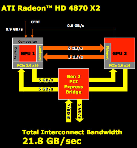
sideport.jpg


Perfect fit for an MCM, does what the northbridge does for Intel quad cores, if I'm not mistaken. There's also that pesky PLX pci-e bridge/switch chip that I'm sure they'd love to get rid of.
 
They don't need to MCM and figure out how to make two GPU chips act as one.. Just use the Hydra chip onboard instead of a PLX switch. Jeez.
 
Back
Top