AMD: R8xx Speculation

How soon will Nvidia respond with GT300 to upcoming ATI-RV870 lineup GPUs

  • Within 1 or 2 weeks

    Votes: 1 0.6%
  • Within a month

    Votes: 5 3.2%
  • Within couple months

    Votes: 28 18.1%
  • Very late this year

    Votes: 52 33.5%
  • Not until next year

    Votes: 69 44.5%

  • Total voters
    155
  • Poll closed .
Question to all:

Do you think there could be a simultaneous launch of both a 5850X2 and a 5870X2 this time?

Is there going to exist a 5850X2 in the first place? Will it be a sinlge vendor exclusive deal like Sapprire's 4850X2 or will we see versions of it from most manufacturers?

I doubt the 5850X2 exist as a SKU at this moment.
 
Question to all:

Do you think there could be a simultaneous launch of both a 5850X2 and a 5870X2 this time?

Is there going to exist a 5850X2 in the first place? Will it be a sinlge vendor exclusive deal like Sapprire's 4850X2 or will we see versions of it from most manufacturers?

I doubt if it will be launched simultaneously with 5870x2.
 
Bandwidth limited?
128bit w/ maybe 5ghz GDDR5 so 80GBps max, most likely it will have slower memory though.
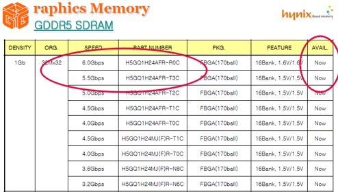
And what if ... (PDF)

Hynix3Q09.png


HD 5600 = GDDR5 4.0Gbps - 4.5Gbps ?
HD 5800 = GDDR5 5.0Gbps - 5.5Gbps ?
HD 5890 = GDDR5 6.0Gbps ?
 
Last edited by a moderator:
6.0Gbps doesn't seem like a worthwhile tradeoff for the ~25% extra power it'd use compared to 5.5Gbps RAM.

Juni XT should still use cheaper RAM, preferably 4-4.5Gbps, but this time perhaps with a much milder underclock. I don't see why you'd wanna go over 4.5 for a $1XX card that would be slashed to $100 in time (which might be 6 months if nVidia has a souped up midrange GD3/5 part with a 256-bit bus ready by then)
 
IIRC HD4870 wasn't exactly bandwidth starving, so there's "spare" membandwidth when you go down before you start doing seriously bad things to your performance?
Correct but how much IPC do you think AMD/ATi was able to do with Juniper? Maybe 10%? We aren't talking about a huge impact with less than 80GBps of bandwidth but I relooked at that 4870/4850 underclocking comparison last night and it was pretty interesting.

I was under the impression that the 181mm2 juniper had a 192 bit bus.
I thought someone had confirmed 4 ICs on top and 4 on the back?
Also, that would greatly increase performance over RV770, more than 5-10%, which isn't what is being reported...

And what if ... (PDF)

Hynix3Q09.png

Tchock said what I would have replied...
 
TSMC's 40nm tech was at 30% yield at Q1 (unrealeased in the market but not what TSMC mean) and 60% at Q2, it logical to expect something 75% if all goes according to plan in Q3 and maybe something better in Q4!

http://www.xbitlabs.com/news/other/...SMC_s_40nm_Yields_Improved_to_60_Company.html

Even the early 40nm RV740 are reaching 850MHz with stock cooler, I don't remember RV770 & RV730 reaching more than 825MHz with stock cooler!
Of cource 850MHz is not ideal scaling but the 40nm had many parametric problems in Q1 2009, things will get better!

RV790 is another discussion, same design as RV770 and ATI could spend all their time to focus how to increase the clocks (they used after all decoupling capacitors technique (+9% in the die space, peripheral zone...)

But 40nm in no way can hit 1GHz (overclocked...) without dec. cap tech. (and i think ATI for this launch will not use this techinique)

BSN is saying 5870 399$, but also they are saying that RV870 is bigger than R600 (so more than 420mm2) which is bs!

Didn't ATI learned their lesson with R600?

When RV790 launched i was forecasting 300$ 300mm2 (+-5% die space) for (32ROPs/64TUs/1280SPs )

or 640SPs at around 2X the core clock, yes like NV did...)

If ATI don't separate from the TU and clock higher the SPs, a DX11 RV770 X2 (32ROPs/80TUs/1600SPs) would be 350mm2 in the best case scenario imo!

I can't see ATI pricing 300$ for a +350mm2 part (AMD needs cash..., and ATI must capitalise the fact the it will have better DX11 avaliability than NV in Q4 2009, if NV launch DX11 in 2009...)

I think ATI should go to 32ROPs, the timing is good (GDDR5 sudden increase(4870 doesn't need 3,6GHz and it was their first GDDR5 design) + we still have many games coming that ROPs are important, example:Dante's Inferno previous game Dead space...)

Also the GT200 design to claim performance leadership from 4890, it helps it that it has 32ROPs, if ATI go to 32ROPS can cause extreme financial problems to NV until NV has GT300, even the DX11 5850 (1280SPs) will be faster than DX10 GT285! if the design is 1600SP even a DX11 5830 will be faster than GTX285!

(Maybe ATI is leaving something (32ROPs) for the future, but for me it is bad strategy this particular timing...

So we are back at the poster, did high end competition part means 5850?
Certainly the 5850 will be high end in relation with the DX10 line up but i doubt powercolor used that way the notion and usually in such contests they give away the higher-end parts like 5870!

It is so difficult to make GPU predictions, so anything can happen...
 
I thought someone had confirmed 4 ICs on top and 4 on the back?
Also, that would greatly increase performance over RV770, more than 5-10%, which isn't what is being reported...

We know there are 4 chips on the back, but I don't remember seeing the front, where there could be 8; which would be consistent with a 192-bit bus.

But I don't see why that would imply considerably higher performance than RV770. Assuming faster memory, there would be pretty much the same amount of bandwidth as the HD 4870, and since we're hearing there are 800SPs...
 
But I don't see why that would imply considerably higher performance than RV770. Assuming faster memory, there would be pretty much the same amount of bandwidth as the HD 4870, and since we're hearing there are 800SPs...
Bandwidth isn't bottleneck for HD4870. It has 125% more bandwidth than HD4770, but only 20% more performance when using MSAA 4x.

/ed.: Another exmple: both HD4870 and HD4890 have the same bandwidth, but HD4890 is 11-12% faster (while the core clock is 13% faster). That proves, that even HD4890 isn't bottlenecked by its bandwidth.
 
We know there are 4 chips on the back, but I don't remember seeing the front, where there could be 8; which would be consistent with a 192-bit bus.

But I don't see why that would imply considerably higher performance than RV770. Assuming faster memory, there would be pretty much the same amount of bandwidth as the HD 4870, and since we're hearing there are 800SPs...

More ROPs, similar bandwidth to RV770, architectural tweaks, better(?)/more complex scheduler but same performance as Rv770?
Doesn't seem worthwhile for little to no performance gains.
 
ed.: Another exmple: both HD4870 and HD4890 have the same bandwidth, but HD4890 is 11-12% faster (while the core clock is 13% faster). That proves, that even HD4890 isn't bottlenecked by its bandwidth.
Good point sir.
Elsewhere I made the comment that a 5870 might be bandwidth limited since they are doubling the specs of the card but only, potentially, increasing bandwidth by 39%, if 5ghz GDDR5 is used. In regards to your example, this may not be the case.
 
Last edited by a moderator:
Bandwidth isn't bottleneck for HD4870. It has 125% more bandwidth than HD4770, but only 20% more performance when using MSAA 4x.

/ed.: Another exmple: both HD4870 and HD4890 have the same bandwidth, but HD4890 is 11-12% faster (while the core clock is 13% faster). That proves, that even HD4890 isn't bottlenecked by its bandwidth.

HD4870 isn't bandwidth-limited, but 4850 is. See here, a comparison of 4850 and 4870 with the same core frequency but 1.86GT/s GDDR3 on one side and 3.6GT/s GDDR5 on the other: http://www.behardware.com/articles/726-4/radeon-hd-4800-s-gddr5-an-advantage.html

And the memory clock speeds went up on HD4890, from 3.6 to 3.9GT/s. Proportionally, it's a bit less than the core clock increase, but still.

And 4770 is bottlenecked. In 1920x1200, it does great without AA, well with 4X, but completely chokes with 8X. See here: http://www.pcworld.fr/article/radeo...as-prix/recapitulatif-des-performances/84031/ (sorry about the French, but the charts speak for themselves). Obviously it's capacity-limited as well, but bandwidth is an issue too, as evidenced by the fact that HD4770 drops behind 4830, which is far slower but has a slightly higher bandwidth, and probably shorter latencies too.

So assuming a 128-bit bus on Juniper and 4GT/s memory, we get 64GB/s, compared to 59.7GB/s on HD4850. That's 7% more, but considering the lower efficiency of GDDR5, let's call it identical. If we assume again that Juniper has 800SPs at 750MHz, we get a part with 20% more raw power, but the same bandwidth as 4850, which is already bandwidth limited.

If Juniper is clocked higher, it's even worse.
 
VRAM capacity is quite limiting at 1920+/AA 8x. If you check test on computerbase, already at 1680/AA 8x the 512MB Radeons ar very close in performance and at 2560/AA 8x HD4850 512MB and HD4870 512MB performs exactly the same(!)

As for HD4770, AA 4x performance is pretty good, while AA 8x performance wouldn't be much better even with higher bandwidth available. I saw two reviews testing this card with AA 8x enabled: PCF.fr (linked by you) and CB.de. The test at CB.de shows, that enabling AA 8x at 1680x1050 doesn't cause any higher performance drop than on HD4870. Enabling AA 8x at 1920x1080 would cause modern game unplayable, even with 5% lower performance drop, which could be achieved using higher bandwidth configuration.

As for HD4850 - I wouldn't call it a limitation - the GDDR5 configuration offers double bandwidth, but ~10-12% performance advantage at the average.
 
FWIW, I'll throw my hat in the ring and say that I feel that leoneazzurro has the right line of thinking on this. For a few reasons.

ATI need to produce two 2+ teraflop cards, and one of them has to be around ~25% faster in games, the reason for that is simple. Its got a $100 (or 50%/33% depending on launch prices) price premium to justify, so a healthy clock bump is the only way that can feasibly happen with no new RAM type to differentiate the parts this time.

That means you're stepping into the 1ghz territory for a 1280 sp part and no matter how successful people claim the 40nm process to be these days I just don't see this happening. Expecting mass availability of a 1ghz GPU on a immature process is just asking for trouble as far as I'm concerned, there's too much room for problems.

If the part is a 1600 SP model then all those worries go away, you can have a very reasonably clocked 5850 and should be able to offer the 5870 with a decent performance boost without getting into the 900mhz/1ghz clock territory. When Hemlock arrives on the scene ATI will have every opportunity to market a 5 (!) teraflop card to spoil Nvidia's launch.

Its just a bit of fun for me but that's the way I see it unfolding anyway.
 
TSMC is forecasting 32nm at Q1 2010 and 28nm at Q4 2010 (the dates are for partners to have products in the market. (we will see execution...) (also the recent delay of the PCI-Express 3 standard, is not good news for the Q4 2010 time...)

I am not sure but i think ATI de-emphasized the need for 32nm and they will focus on 28nm
(the main reason for me that ATI said that, is because GlobalFoundries is going to have in Q4 2010 (best case scenario, probably Q1 2011) risk production capability (don't compare the timing of the AMD's 32nm CPU upcoming products, it is completely different process...) (but we will see..., +1 year is a long period for ATI to stick to 40nm...)

The possibilities are so many for ATI & NV to have new HD6XXX/HD7XXX products (ATI's case) in the next year (until Q4 2010), that any prediction is essentially meaningless...


I see some members are trying to correlate if the upcoming designs will be bandwidth limited, comparing the memory controllers of older products, trying to make the equation...

The memory controller will be new in the DX11 products just like it was different in the HD2000/HD3000/HD4000 series (even these was same DX10) (1 year and 1 quarter period... Q1-Q2 2007 - Q2-Q3 2008),

also i would like to point out that despite my expectations, RV740's memory controller is better than RV770 memory controller (RV770 mem. con. was their first GDDR5 based design and i think that the efficiency is based also in the factor that the GPU must scale perf. with GDDR5 (256bit mem. con., 200$GDDR3->300$GDDR5 at launch) so i think it was also a design choice...

The memories of the 4770 (in most AIBs) are 4GHz (effective) (3,2 GHz is the standard clocking ATI is giving) Try overclocking them at 4GHz and see the differences in perf... (for some games also 512MB is a problem depending the resolution and the anti-aliasing level...)

But anyway let's not devote time if the RV740 memory controller is better than RV770...

Because, like i said the memory controller will be a different one in the new parts...

my expectation is that for 800MHz GPU (16/32 ROPs) a good speed will be 4800 MHz (effective) (So they will need 5Gbps ICs) (128bit/256bit mem. con.)

The lower end part with the 128bit memory controller cannot use 5Gbps ICs (too expensive...) so it will use 4,5Gbps ICs, so it will be a little bit bandwidth limited...

But i can't prove anything, just my expectation...

Actually there is even the chance that the higher part (256bit mem. con.) will use
4,5Gbps ICs and the lower part (128bit mem. con.) 4,0Gbps ICs. (standard configurations...) but i don't like that scenario, i prefer the above one...
 
Just a clarification because i can't edit...

TSMC revised to +1 quorter the roadmap (and i don't think that 32nm will be desirable in Q2 2010, but will see...)

And for Globalfoundries i meant 28nm risk production capability in Q4 2010 (best case scenario of cource...)
 
So who will buy the 5,5Gbps & 6,0Gbps GDDR5 from Hynix ?
If Hynix produce it, it's because someone wants it.
Surely Hynix won't pile up these vram in a warehouse.
There are only two possibilities: AMD or Nvidia.
 
ATI need to produce two 2+ teraflop cards, and one of them has to be around ~25% faster in games, the reason for that is simple. Its got a $100 (or 50%/33% depending on launch prices) price premium to justify, so a healthy clock bump is the only way that can feasibly happen with no new RAM type to differentiate the parts this time.
I don't really agree with that. There needs to be some reasonable difference, yes, but about 20% would be enough. There will always be people who just buy the fastest. Just look at GTX 275 vs . GTX 285, there is maybe if you're lucky a 10% performance difference but the GTX 285 costs almost 100$ more.
So 785Mhz and 950Mhz 1280SP parts would still do it. And I just can't see 950Mhz as a big problem, surely 40nm process even if not very mature should reach at least same frequencies as 55nm.
A 1600SP part would make it possible to introduce an even faster model later though presumably.
 
Back
Top