The slide clearly communicates that CoD will be slower hence the use 0.9x. Even if you interpret to say 0.9x as fast that translates to CoD being slower. Math isn't that difficult for some time grasp is it? The chart also clearly communicates CoD is slower in a visual manner.
You are using an out of date browser. It may not display this or other websites correctly.
You should upgrade or use an alternative browser.
You should upgrade or use an alternative browser.
RDNA4
- Thread starter Frenetic Pony
- Start date
AMD have various patches for things like gfx12 dcc (delta colour compression) and VCN 5 (video block) on the way. Hope they'll have Xilinx IP this gen, their AV1 encoding quality was very impressive in the MA35D and would be a significant step up

PowerColor’s “Next-Gen” AMD Radeon GPUs To Work With NPUs To Reduce Power Consumption While Gaming
PowerColor integrated NPU to Radeon GPU. (Still developing)
Through AI, they claim power consumption deceased 22%. More saved than AMD Power Saving
There's no way AMD are going to integrate Xilinx's media processor implementation. Integrated media processor functionality is never going to match up to the quality of contemporary dedicated media processors so if there are potential customers out there who want better video playback/recording then dedicated media accelerators will meet their needs/requirements better than an integrated implementation ...AMD have various patches for things like gfx12 dcc (delta colour compression) and VCN 5 (video block) on the way. Hope they'll have Xilinx IP this gen, their AV1 encoding quality was very impressive in the MA35D and would be a significant step up
Frenetic Pony
Veteran
For products "not coming until next year" AMD sure likes patching software support for them a whole lot: https://www.phoronix.com/news/AMDKFD-GFX12-Support
I.E. I'm guessing laptop versions will be out at CES, but they'll tease RDNA4 desktop/announce press conference at the Zen 5 availability launch next month, then launch RDNA4 desktop in August.
I.E. I'm guessing laptop versions will be out at CES, but they'll tease RDNA4 desktop/announce press conference at the Zen 5 availability launch next month, then launch RDNA4 desktop in August.
Last edited:
An improvement with GFX12 DCC over prior generations is that compression is enabled for formats (R32/R64) that support atomic operations. Before DCC resources would decompress if atomic operations were used with those formats. I think some of us already has an idea with where exactly things are going with Nanite's virtualized geometry visibility buffer ...
https://wccftech.com/amd-patent-uni...pproach-future-rdna-architectures-three-dies/
AMD's patent filing reveals that the company is exploring "multi-chiplet" GPU design options, suggesting that next-gen RDNA architectures might feature massive changes. The patent describes the use of three different "modes" of chiplet utilization, where the difference lies in how resources are allocated and then managed ahead. The patent reveals three different models, with the first one being the "single GPU" mode, which is quite similar to how modern-day GPUs function. All the onboard chiplets will act as a single, unified processing unit, with resources shared in a collaborative environment.
it works in three mode:
first is single GPU" mode, which is quite similar to how modern-day GPUs function. All the onboard chiplets will act as a single, unified processing unit, with resources shared in a collaborative environment.
The second mode is called the "independency mode", where individual chiplets would act independently, responsible for their functions through the dedicated front-end die responsible for scheduling tasks for its associated shader engine dies
The third mode is the most optimistic of them all and is called the "hybrid mode" where chiplets can act independently and co-exist as well. It leverages the benefits of both unified and independent processing, offering scalability and efficient resource utilization.
Last edited:
The patent mentions vertical stacking of FE and SE dies which seems ideal.
It might look like this.
Top: Shader Engines + L1 cache
Middle: Front End + L2 cache
Bottom: I/O + memory controllers + L3 cache
The multiple software visible FE configuration seems awkward for gaming APIs and a driver developer’s worst nightmare so I’m guessing that will be reserved for more custom use cases. Multiple hardware FEs may be needed anyway to co-ordinate instructions from the primary FE and provide more surface area for stacking SEs.
Frenetic Pony
Veteran
I suspect the stacking is never going to happen, that just sound like a heat sandwich and there's already headaches just over backside power delivery, let alone trying to stack cache and logic on top of each other. The "3d chip!" seems like an engineer that's never had to deal with chip practicalities dream, and it seems likely to remain that way.
Frenetic Pony
Veteran
Isn't this patent obviously about the MI300X? Which is in production and available today?
No, this is for RDNA, and most likely 5. The "front end" here is the section that's the hardest to split up into multiple dies, as that's generally a serial list of commands for the GPU that then gets split up into multiple commands for the shader engines (etc.) from this serial list. It seem AMD has been trying to split this part up for years, failed to do so for RDNA4, but may have finally succeeded for 5.
This would allow the tapeout of a single type of die for most of a gaming GPUs logic, which could then be copied and packaged as many times as desired. Example given, say two 16CU "shader engines" per "front end", copied 3 times, would give you the same amount of compute units as a 7900XTX.
The patent doesn't show the memory bus chiplets, but of course AMD already cracked that problem. So you'd have X memory bus chiplets, "multimedia/mode selector" chiplet, and then X front end/shader engine chiplets.
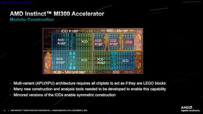
MI series has a more complex layout, you can take a look at just one of the block diagrams here:
You're right the patent explicitly talks about graphics, so I shouldn't say the patent is specifically about MI300X - but as you point out scaling graphics that way is a much harder problem than compute, and the patent doesn't actually offer any solution to *how* to distribute the work and it only mentions the word triangle once... it's basically "and then, magic happened" - if they have solved that problem (which is very possible!) then that would be in a separate patent.
I was personally involved in a patent (apparently not public yet, filed ~1.5 years ago, regarding Imagination's DXT texture unit) where the patent team ended up creating two patent filings for more or less the same invention, one for "graphics" and one for "compute" with very minor differences between the two. I wouldn't be too shocked if there was a "compute" equivalent to this patent (which might not be publicly available yet) which is basically MI300X, and this is a similar patent created to cover all bases... hard to say for sure.
What do you think is different for MI300X though, besides graphics vs compute? It looks like it's literally describing MI300X in every way to me. The "Front End" dies are the IODs and the "Shader Engine" dies are the XCDs. The CCDs are the Zen CPUs for the MI300A (rather than MI300X) which wouldn't be described by this patent. It talks about how it can be used both working together or individually as if it was multiple separate GPUs, which is indeed something MI300X can do.
And MI300X very much is doing 3D stacking (of the XCDs on the top of the IODs) and it's apparently not melting, it's a very cool design in my opinion") Whether it makes sense for consumer RDNA is a question of cost, and as you say, whether they have managed to solve the "distribute graphics work across multiple front-ends"!
Whether it makes sense for consumer RDNA is a question of cost, and as you say, whether they have managed to solve the "distribute graphics work across multiple front-ends"!
I was personally involved in a patent (apparently not public yet, filed ~1.5 years ago, regarding Imagination's DXT texture unit) where the patent team ended up creating two patent filings for more or less the same invention, one for "graphics" and one for "compute" with very minor differences between the two. I wouldn't be too shocked if there was a "compute" equivalent to this patent (which might not be publicly available yet) which is basically MI300X, and this is a similar patent created to cover all bases... hard to say for sure.
What do you think is different for MI300X though, besides graphics vs compute? It looks like it's literally describing MI300X in every way to me. The "Front End" dies are the IODs and the "Shader Engine" dies are the XCDs. The CCDs are the Zen CPUs for the MI300A (rather than MI300X) which wouldn't be described by this patent. It talks about how it can be used both working together or individually as if it was multiple separate GPUs, which is indeed something MI300X can do.
And MI300X very much is doing 3D stacking (of the XCDs on the top of the IODs) and it's apparently not melting, it's a very cool design in my opinion
Whether it makes sense for consumer RDNA is a question of cost, and as you say, whether they have managed to solve the "distribute graphics work across multiple front-ends"!Frenetic Pony
Veteran
Indeed, I've no idea how they're proposing front end splitting works in any detail. There was an earlier patent about distributing work between geometry engines, but it's assumed that was to do with the cancelled RDNA4 chiplet architecture.
They mention multiple strategies, one "front end die" gets mapped to all shader engine dies, multiple front end dies split the front end work evenly and only process commands for their corresponding shader engines, or that two front end dies work in tandem. It seems like they're trying to cover a whole lot bases with this patent. I'm unsure if they're just trying to make the patent as broad as possible or if they're actually trying multiple strategies and don't know which ones will work yet.
As for stacking, as long as it's low power like an IOD you can stack logic on top of it if you really need to, but I'm worried stacking 3, including front end which is logic, would just run into way more trouble than it's worth.
the patent doesn't actually offer any solution to *how* to distribute the work
It does actually. One of the modes has one “master” FE face off to the host CPU and handle distribution of work to the other FEs and SEs. This is similar to how monolithic GPUs work today. The question is can they do it with reasonable latency and power consumption.
Frenetic Pony
Veteran
edit - woops misread it
Last edited:
Tkumpathenurple
Veteran
If that would be such a benefit, why haven't AMD done it until this hypothetical scenario?I'll go further and say RDNA5 could have M3's unified register/L1/shared memory.
I'm not trying to be snarky btw, I'm genuinely curious.
It's little low hanging fruit things like this that gives NVidia the market share it has, AMD's HW encoding quality is really bad with either AVC/AV1, encoding anything at twitch standard 6Mbit settings for ex. with either HQ/CBR/VBR in any barely moving image just encodes a bad mix of blurry and blocky image with no detail preservation whatsoever. I'm not even a streamer but sometimes one would like to record stuff for a guide or showing funny stuff, etc. and even simple things like this makes me uneasy about going with AMD next round since very little to nothing has been done to improve their encoding quality, instead they decide to waste a few millions chasing the overblown "AI" bubble.There's no way AMD are going to integrate Xilinx's media processor implementation. Integrated media processor functionality is never going to match up to the quality of contemporary dedicated media processors so if there are potential customers out there who want better video playback/recording then dedicated media accelerators will meet their needs/requirements better than an integrated implementation ...
Similar threads
- Replies
- 70
- Views
- 20K
- Replies
- 32
- Views
- 9K
- Replies
- 36
- Views
- 9K