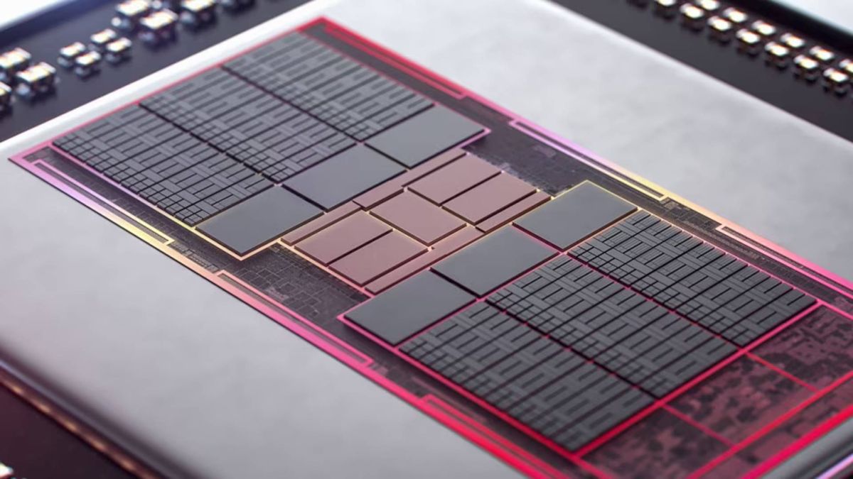
RDNA4

Damn foundry's are pretty greedy, I would have used low-NA EUV at the 8nm node and high-NA at 3nm, but i guess them's the brakes.
It's not really greedy in this case. High NA is going to require extremely high up front investment costs to get the machines in the first place and have fabs modified or more likely built newly to house and run them. This wouldn't be a huge issue if it was just some one time thing, but ASML can only build so many of these machines and it's going to take a good while before any company can buy and install enough of them to really have a high volume manufacturable node using High NA. And this is disregarding the also very tough job and resource investments into designing such nodes in a successful manner.

TSMC's leading edge customers will require very large volumes of chips, so betting big on High NA early on could completely fall apart if they simply dont have enough capacity to serve them for a good while and those machines just sit there producing no chips and thus no returns. Intel is in a bit more fortunate situation in that they can use the slower scale up in volume to still produce chips for themselves, up until they've got enough capacity to open up to external customers.

TSMC's reasoning honestly makes sense here. It's a tricky situation, and one where making a bad bet can incur some pretty devastating financial consequences.
 
N3P ready for tapeouts this year: https://www.anandtech.com/show/2139...nology-on-track-for-mass-production-this-year

Guessing that means RDNA5 will be on N3P, especially considering the apparent per wafer costs associated with TSMC N2.
Seems likely, could even be N3S possibly as N3E/N3P does not scale for SRAM at all and N3S could help with density. RDNA5 is rumoured to come out in H1'25 so N3S would be available by then as well.
Well N2 is gonna be eaten up completely by Apple anyways.
Zen 6 dense/Zen 6c chiplet is apparently one of the first N2 chips as well but likely wafer quantity and yield for larger dies will not be suitable for larger GPUs initially. Perhaps we will see RDNA6 on N2P/A16.
Not even those, they're planning to do even A14 (or whatever they'll end up calling it) with normal EUV and expect it might actually still be cheaper despite multipatterning requirements. Some reports said they might not do High NA before 2030
Actually they haven't committed to anything with A14 yet, they've only said that they are still evaluating but yes it seems likely they will skip it for A14 and will wait. Meanwhile Intel seems to be all in on HNA for 14A
 
Is RDNA5 (or 6) going to get rid of the "Infinity cache", maybe just on mobile/higher end?

I was just looking at Apple M series benchmarks, and 100ns to main VRAM is amazing, and that's just on M1. RDNA3 takes 150ns just to get to MALL, 250ns to get to VRAM. Splitting off Infinity Cache entirely and going large on chip L2 MALL with SRAM chiplet(s) for extreme bandwidth and then skipping directly to on package VRAM would cut latency by a huge amount and power by a decent amount as well, hopefully without oversaturating VRAM bandwidth.

This would mean changing GPU accounting entirely, and the accountants will complain they can't foist off the "cost" of VRAM to board partners and their precious "profit margin" will go down as a result. But if packaging gets cheap enough, which it's definitely heading towards, it's the right engineering decision.
As far as I know, most of the 100ns latency on the M-series chips comes from their memory controller / internal bus design + the inherent latency advantage of LPDDR4x/5 vs GDDR versus the RAM physically being on package. Most of the reason to stack the RAM on top of the chip (cell phone/tablet style) or on package (Apple M1 / Intel Lunar Lake style) is just the reduced PCB area requirements.

I'm sure you can probably push the hairy edge of latency/frequency a bit more by putting the RAM on package, but that's not likely where the majority of the gains are. Plenty of LPDDRx implementations have the memory on the PCB as well.

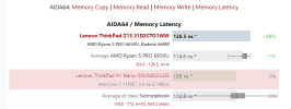
If you scroll down to the AIDA64 latency tests, we're already at 105ns for main memory with creaky old LPDDR4x (same as the Apple M1 non-pro) on the Lenovo ThinkPad X1 Nano-20UN002UGE with Intel Core i7-1160G7, and it's not integrated onto the package, it's on the PCB.


1716417133345.png
 
Most of the reason to stack the RAM on top of the chip (cell phone/tablet style) or on package (Apple M1 / Intel Lunar Lake style) is just the reduced PCB area requirements.

There are also very real power savings because of lower lane capacitance, but the time saved by the lower RC delays is minimal.
 
Is RDNA5 (or 6) going to get rid of the "Infinity cache", maybe just on mobile/higher end?

I was just looking at Apple M series benchmarks, and 100ns to main VRAM is amazing, and that's just on M1. RDNA3 takes 150ns just to get to MALL, 250ns to get to VRAM. Splitting off Infinity Cache entirely and going large on chip L2 MALL with SRAM chiplet(s) for extreme bandwidth and then skipping directly to on package VRAM would cut latency by a huge amount and power by a decent amount as well, hopefully without oversaturating VRAM bandwidth.

With new manufacturing technologies, SRAM is becoming more expensive. Making big on-die cache is expensive and is gettin more expensive. And also, making the L2 bigger also makes it slower.

The only way to have relatively cheap big cache is to put that cache on a separate die which is made on older manufacturing process(what AMD did in RDNA3). But that increases latency and power.

One reasonable direction might be keeping the outer level cache on a separate die, but trying to minimize the overheads of the die-to-die traffic, for example by integrating the dies vertically, cache die below or above the logic die. Something similar than what AMD did on the Zen-3D/v-cache.


Apple has fast access to their DRAM because the memory controllers on the same die (which is costly on new mfg processes) and also because they use LPDDR line of memory which is more latency-optimized, less bandwidth-optimized than GDDR line of memory.

And Apple can afford to pay for the cost of having the memory controllers on-die because they are selling their products at very high price, they have good margins anyway. Consumer GPUs have much less margins than Apple products and AMD has to try to save more on mfg costs.
 
One reasonable direction might be keeping the outer level cache on a separate die, but trying to minimize the overheads of the die-to-die traffic, for example by integrating the dies vertically, cache die below or above the logic die. Something similar than what AMD did on the Zen-3D/v-cache.
AMD are already doing this with MI300.

This definitely feels like the way forward if it's decided that large L2/L3 caches are important to have. At least for higher end GPU's.
 
The only way to have relatively cheap big cache is to put that cache on a separate die which is made on older manufacturing process(what AMD did in RDNA3). But that increases latency and power.

There's this interesting concept some company is selling the... rights to, engineering services, some sort of thing like that as they're not a foundry. Anyway it's a stacked on die GDDR ram cache kind of like modern EDRAM. The point they're selling for is AI accelerators, but it could work for other things. 256mb(+?) of GDDR seems cheaper than the equivalent SRAM as well.
 
Makes zero sense and seems either fake or mistranslated. N48's specs are basically 2 x N44 but it would make zero sense to do an MCM instead of a separate die.
Only way it makes a bit of sense would be if the entire lineup was meant to be MCM and N44 was basically the 'base' design with a single compute tile. IE, N44 == 1x, N48 == 2x, cancelled Navi 4c/41 is 4x or 6x, but there was some intractable problem like power consumption of the intra-tile links that are bad but not a showstopper with only one link in play for a hypothetical tiled N48 design, but enough to kill the larger part entirely, especially if the intra-tile links for more than 2 tiles ended up having to be a mesh layout.

But I agree that the entire situation sounds unlikely.
 
Not sure what the exact packaging is. But the cancelled one was supposed to be each shader engine was it's own die. If this is just two dies that are more like complete, self contained GPUs (with/out their own IO? Seperate IO dies? whatever) then this could be a different non cancelled arch.

They might still have skipped most of it in favor of advancing RDNA5 over things like the rise of AI. RDNA5 with a dedicated matrix pipe is useful for selling as a "cheap" inference card, especially if you can separately tailor the amount of bandwidth to it (gaming GPU wants cache, inference wants bandwidth to VRAM), which RDNA4 wouldn't be nearly as useful for.
 
Only way it makes a bit of sense would be if the entire lineup was meant to be MCM and N44 was basically the 'base' design with a single compute tile. IE, N44 == 1x, N48 == 2x, cancelled Navi 4c/41 is 4x or 6x, but there was some intractable problem like power consumption of the intra-tile links that are bad but not a showstopper with only one link in play for a hypothetical tiled N48 design, but enough to kill the larger part entirely, especially if the intra-tile links for more than 2 tiles ended up having to be a mesh layout.

But I agree that the entire situation sounds unlikely.
Nah, it is not worth duplicating the "uncore" for each GPU, that's significant wasted area. Rumoured die size of N48 is ~240mm2 vs 130mm2 for N44, which is less than double despite specs being exactly double. If at all this was possible, it would be relatively easy to do a N41/42 even at the cost of additional die area/power (7900 XT/XTX still make good margin despite consuming higher power than Nvidia cards). As per the leaks, Navi 4c was to have separate base dies, GCDs and MCDs.
 
Well that's just further proof of how conniving AMD's secret leak department has gotten. Gotta confuse people as much as possible, while suggesting there's secret clues in there so people will repeatedly look at your posts hoping to unlock the truth. I know it may look like some lazy engagement scam, but no, it's really AMD playing a masterstroke, just like they did the Navi 10 price jebaiting that totally wasn't them just trying to be greedy and reversing cuz of backlash.
 
i guess the true part wasn't interesting enough to be translated.
The whole post referenced in the tweet says (pick your poison)
Bing (or whatever Edge built in is)
AMD only manufactures the Navi48, which packages a relatively high-end model through the INFO process, while the 44 is a 48-cut chiplet cut in half, which is packaged in a conventional package.
The point of this is to make MCM graphics GPUs ahead of Blackwell.

Google:
AMD only produces the Navi48, a relatively high-end model through the INFO process, a small chip of 44 and 48, then uses a traditional package.
The meaning of this is that MCM's graphics GPU was made before Blackwell.

Baidu:
AMD only produces Navi48 and packages relatively high-end models through the INFO process. For small chips that are cut in half for 48, traditional packaging is used.
The significance of doing this is to make the MCM graphics GPU before Blackwell.

DeepL:
AMD only produces the Navi48, a relatively high-end model packaged through the INFO process, and the 44 for the smaller chips cut in half for the 48, in a conventional package.
The point of this is to make MCM graphics GPUs in time for Blackwell.

Systran:
AMD only makes Navi48, which is packaged in a relatively higher-end model using INFO technology, and 44 is a small chip cut in half by 48, using traditional packaging.
The significance of this is to make the graphics GPU of MCM before Blackwell.

edit:
Later in thread (Baidu translation since had it open)
It may also not require bridges or advanced packaging, it can simply be cut in half
 
Back
Top