RDNA4

Known:
This year
GDDR7
Raytracing Traversal (similar performance to Intel/Nvidia)
Powerdraw is fixed, very high clockspeeds

Leaked?(by you know who, plus some dumb AMD engineer on a youtube comment)
Announcement in H1, maybe Computex
Big chip is in this time, likely stacked SRAM and such
Big chip is really expensive, stupid big, tons of power draw, there solely for PR purposes, >$1k
$1k >= chip is more mainstream high end.
 
This post’s accuracy is not substantiated. Exercise discretion and wait for verified sources before accepting its claims.
Maybe.
Raytracing Traversal (similar performance to Intel/Nvidia)
Yes but not quite.
Powerdraw is fixed, very high clockspeeds
Seems so.
Announcement in H1, maybe Computex
Yea.
Big chip is in this time, likely stacked SRAM and such
Dead.
Big chip is really expensive, stupid big, tons of power draw, there solely for PR purposes, >$1k
It's dead, jim.
$1k >= chip is more mainstream high end.
Oh, any stacked Si spam part will be far above $1k.
You'll have to wait for Navi50 for that, which also gonna double as a DC GDDR-based PCIe stick.
 
Guesses:

12WGP, 64bit bus, monolithic, 8gb ram, 32mb SRAM LLC, 3.2ghz =<, 4060, $199

32WGP, 256bit bus, 16gb ram (28gbps), 64mb LLC, 3.1ghz, 4080 $699
28WGP, 192bit bus, 12gb ram, 48mb LLC, 2.9ghz, 4070ti, $499
24WGP, 128bit bus, 16gb ram, 32mb LLC, 2.7ghz, 4070, $399
64WGP, 384bit bus, 24gb ram, 192mb LLC, 3.1ghz, 50% faster than 4090, $1599
56WGP, 320bit bus, 15gb ram, 80mb LLC, 2.8ghz, 20% faster than 4090, $1k

Maybe.

Yes but not quite.

Seems so.

Yea.

Dead.

It's dead, jim.

Oh, any stacked Si spam part will be far above $1k.
You'll have to wait for Navi50 for that, which also gonna double as a DC GDDR-based PCIe stick.

Big chip is from our favorite resident leaker, and a second source, who is a confirmed AMD engineer that got stupidly mad on a youtube comment. MLID is just some youtuber after clicks. That being mr resident leaker has kinda been circumspect around a "big chip" other than it being in the cards somewhere soonish.
 
This post’s accuracy is not substantiated. Exercise discretion and wait for verified sources before accepting its claims.
Big chip is from our favorite resident leaker, and a second source, who is a confirmed AMD engineer that got stupidly mad on a youtube comment.
N4C's do not exist anymore.
It was a chtonic 120+ WGP something on the upper end that was knifed in favour of just fast tracking RDNA5.
4 is like the orphan family now where only 2 out of 7 parts planned survived.
 
N4C's do not exist anymore.
It was a chtonic 120+ WGP something on the upper end that was knifed in favour of just fast tracking RDNA5.
4 is like the orphan family now where only 2 out of 7 parts planned survived.

120??? What would that even be, watercooled 600w at 2.2ghz, maybe more?
I mean, some of the big integrators have gotten air cooling past 450w now, I can see Nvidia pulling up 525w (PCIE5 75w direct and a full 450w connector) for Blackwell 5090, just to flex again ($1800 card yaaay)... but who would try anything more, seems out of control.
 
By the looks of the GFX12 LLVM patches so far:

1. No patch having mentioned hardware traversal (yet?); still only image bvh intersect + DS traversal stack instructions * from GFX11.

2. The architecture has the concept of multiple AIDs, though whether any models with multiple AIDs has survived the alleged chop is a separate question…

3. Lots of changes to memory access policy control (SLC/DLC/GLC -> 3-bit temporal reuse hint + 2-bit for scope a la shader-engine/device/system)

4. New WMMA instructions and SWMMAC instructions. Not sure what S stands for in the latter… sparsity? super?

Edit: Somehow `ds_bvh_stack_*` (traversal stack in LDS) is left out for GFX12. An indication of some changes, at least.
 
Last edited:
This post’s accuracy is not substantiated. Exercise discretion and wait for verified sources before accepting its claims.
Will RDNA 4 be topping out at the 400$ tier?
Higher (shouldn't be by much, though, those are mainstream/mobile parts).
 
Based on the rumors/leaks only 2 GPU remain for the RDNA4 lineup, the N44 (IMO most likely the successor of the N33) and the N48. Both are said to be monolithic designs in the lowend (N44) or midrange (N48) class.

But, what if the leaks/rumors about the monolithic designs are not entirely correct?

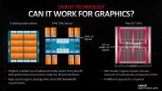
N41 for example was a design with 3 x [chiplets with chiplets], with a two level chiplet-design. Based on some patent drawings the inner level with the /SED/, /memory/ and /CP/ chiplets on top of a bigger base-chiplet and then the outer level with 3 of these base-chiplets forming the N41 GPU, or 2 of these chiplets forming the N42 GPU and 1 chiplet used for the N43 GPU.

Link: https://www.forum-3dcenter.org/vbulletin/showpost.php?p=13374402&postcount=573
the same patent drawing was discussed here in the forum, but I was not able to find the link.

Therefore, for me it seems possible that the inner level of [chiplets with chiplets] was abandoned due to capacity problems but not the outer level with 1-3 chiplets.

N48 could be a “monolithic” chiplet/GPU to replace the N43 chiplet-based design but from my point of view this does not rule out that 2-3 N48 could still be used for some sort of highend GPU’s as long as the distributed command processor and architecture, designed for RDNA4 work as intended.

any thoughts?
 
N48 could be a “monolithic” chiplet/GPU to replace the N43 chiplet-based design but from my point of view this does not rule out that 2-3 N48 could still be used for some sort of highend GPU’s as long as the distributed command processor and architecture, designed for RDNA4 work as intended.
No you can't, N4m's aren't made for that at all.
Very simple products overall.
 
RDNA 4 continues AMD’s GPU ISA evolution. Software prefetch and more flexible scalar loads continue a trend of GPUs becoming more CPU-like as they take on more compute applications. AI gets a nod as well with FP8 and sparsity support. Better cache controls are great to see as well, and more closely match the ISA to RDNA’s more complex cache hierarchy.

Finally, remember nothing is final until a RDNA 4 product is released. All the information here is preliminary.

 
What I don't get about the new chiplet patent (cancelled arch) is why go for the hardest thing first, which is work distribution and coordination independence for each chiplet?

Why not just split out shader engines to their own chiplets then have unique command processor/etc. etc. per SKU. You still get most of the benefits of chiplets cost wise, even if you need to plan/build each specific GPU separately. Why go for the hardest possible arch first?
You see CP itself as a separable freestanding block. But the graphics pipeline is a monolithic state machine spanning from the central CPs & geometry processor, shader dispatch network, to per shader engine resources like rasterisers, export buses/caches and render backends. It is a blend of control and data paths and plenty of intermediate state, all of which are outside of the R/W cache hierarchy. Many of these do not naturally enjoy a clean chop like how memory channels or screen-space partitions do.

Imagine trying to break a CPU core front-end and several execution clusters off as individual chiplets. Might as well do the hardest thing, aka going multi-core with complete core(s) as chiplets & inevitably calling for complicated things like cache coherency and DVFS management.

Edit: Doing the “hardest thing” first, you get scalable clean chops (chiplets) using solely standard IP interfaces, i.e., blocks can coordinate themselves solely through the system/device memory hierarchy. (e.g., IMG “Multi-Core” GPU) Meanwhile, going for a compromise and one might end up with chiplets having lots of one-off custom interfaces to serve graphics pipeline internals.
 
Last edited:
You see CP itself as a separable freestanding block. But the graphics pipeline is a monolithic state machine spanning from the central CPs & geometry processor, shader dispatch network, to per shader engine resources like rasterisers, export buses/caches and render backends. It is a blend of control and data paths and plenty of intermediate state, all of which are outside of the R/W cache hierarchy. Many of these do not naturally enjoy a clean chop like how memory channels or screen-space partitions do.

Imagine trying to break a CPU core front-end and several execution clusters off as individual chiplets. Might as well do the hardest thing, aka going multi-core with complete core(s) as chiplets & inevitably calling for complicated things like cache coherency and DVFS management.

Edit: Doing the “hardest” thing, you get scalable clean chops (chiplets) using solely standard IP interfaces, i.e., blocks can coordinate themselves solely through the system/device memory hierarchy. (e.g., IMG “Multi-Core” GPU) Meanwhile, going for a compromise and one might end up with chiplets having lots of one-off custom interfaces to serve graphics pipeline internals.

I’m no hardware engineer but it seems the path of least resistance would be to prove out CP work distribution on die first before splitting into multiple dies. If it doesn’t work on-die it’s definitely not going to work on-package.
 
Back
Top