Official PS3 Thread

Status
Not open for further replies.
Let's clarify that guesstimate diagram once more. I'm ignoring the integer units for now. I also don't care about the Processor Elements because they seem to be only for higher level organisation of the layout -- it's the APUs that matter here. I'm assuming Visualiser has half the number of APUs because it also has dedicated pixel rasteriser hardware and the eDRAM.


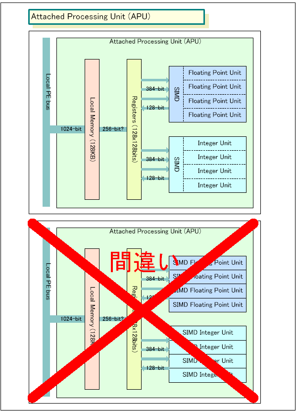
APU = each APU has 4 SIMD units, each SIMD unit has 4 FMAC units, each FMAC (multiply & accumulate) is 2 ops, so each APU does 32 ops per cycle.


Cell: 32 APUs = 1024 ops/cycle. At 1 GHz that's 1 TFLOPS.
Visualiser: 16 APUs = 512 ops/cycle. At 1 GHz that's 512 GFLOPS.


Those figures not including the rest of the hardware (FDIV and other more specific units). Who needs 2 or 4 GHz? 8)


(Putting this much ALUs and cache into a chip means that at 2+ GHz it gets so hot the PS3 comes inside a Sony fridge. The toaster pic ain't a complete joke...)


All excluding the math IMHO!
 
so megadrive is wrong you are trying to say so if you have a 1ghz gpu for the ps3 you can get 512 gflops not 128 glops

edit: so i guess you dont need a 4 ghz gpu
 
Japan's Toshiba Corp. and Sony Corp. will present one of the more widely anticipated papers at the event, entitled “Highly Reliable Cu/Low-k Dual-Damascene Interconnect Technology with Hybrid (PAE/SiOC) Dielectrics for 65nm-Node Performance eDRAM

http://eetimes.com/semi/news/OEG20030530S0040

This 65 nm eDRAM maybe could be used in PS3? And what do you guys think we will find out about Cell at IEEE this year?
 
wait a minitue, qwerty, I said that IF Cell with 32 APUs at 4 Ghz only got 1 TFLOP, then Visualizer with 16 APU at 1-2 GHz would only get 128-256 GFLOPs.

(start with 1 TFLOPs, then half and half again = 256 or half one more time gives 128)


BUT, if it is true that a 1 GHz Cell with 32 APU gets TFLOPs then Visualizer at 1 GHz with 16 APUs would get 512 GFLOPs.


Guys, is there anything to support Gunhead's theory that 32 APUs clocked at 1 Ghz will give 1 TFLOP performance? I think it would be neat if it could. because then, with .065 process technology, it might be able to be clocked at 2-4 GHz, giving us 2-4 TFLOPs which would be quite nice. :)
 
APU = each APU has 4 SIMD units, each SIMD unit has 4 FMAC units, each FMAC (multiply & accumulate) is 2 ops, so each APU does 32 ops per cycle.

Guys, is there anything to support Gunhead's theory that 32 APUs clocked at 1 Ghz will give 1 TFLOP performance?

Well besides, it gives 1 TFLOPS at 1 GHz, there is also the large number of registers.

But to accomadate 4 SIMD units, in that one APU, you have to also remember to have another 4 units for the interger part. So basically you are increasing the size of each APU by quite alot, and when you have 32 of these things, it carries alot of weight. So who knows, maybe clocking the thing at 1 GHz with 8 SIMD units in each APU is more far fetch than 4 GHz with 2 SIMD units in each APU :?:

And then you have to issue instructions to those 8 SIMD units too.

The patent did make room for more floating point and integer units. So it is open for speculation ;)
 
V3 said:
But to accomadate 4 SIMD units, in that one APU, you have to also remember to have another 4 units for the interger part. So basically you are increasing the size of each APU by quite alot, and when you have 32 of these things, it carries alot of weight. So who knows, maybe clocking the thing at 1 GHz with 8 SIMD units in each APU is more far fetch than 4 GHz with 2 SIMD units in each APU

With 100M gate devices already being designed for the 90nm step; I'd say it's much more likely that the design will be clocked at 1GHz and use concurrency rather than clock scaling to extract preformance.
 
With 100M gate devices already being designed for the 90nm step; I'd say it's much more likely that the design will be clocked at 1GHz and use concurrency rather than clock scaling to extract preformance.

With 8 SIMD units, each APU become really complex. You need to issue 8 instructions to get the optimal performance. That will be some kind of VLIW/SIMD machine for each APU.

Lets revisit the patent again.

[0065] PU 203 can be, e.g., a standard processor capable of stand-alone processing of data and applications. In operation, PU 203 schedules and orchestrates the processing of data and applications by the APUs. The APUs preferably are single instruction, multiple data (SIMD) processors. Under the control of PU 203, the APUs perform the processing of these data and applications in a parallel and independent manner. DMAC 205 controls accesses by PU 203 and the APUs to the data and applications stored in the shared DRAM 225. Although PE 201 preferably includes eight APUs, a greater or lesser number of APUs can be employed in a PE depending upon the processing power required. Also, a number of PEs, such as PE 201, may be joined or packaged together to provide enhanced processing power.

[0068] FIG. 4 illustrates the structure of an APU. APU 402 includes local memory 406, registers 410, four floating point units 412 and four integer units 414. Again, however, depending upon the processing power required, a greater or lesser number of floating points units 512 and integer units 414 can be employed. In a preferred embodiment, local memory 406 contains 128 kilobytes of storage, and the capacity of registers 410 is 128.times.128 bits. Floating point units 412 preferably operate at a speed of 32 billion floating point operations per second (32 GFLOPS), and integer units 414 preferably operate at a speed of 32 billion operations per second (32 GOPS).

After suggesting the APU being SIMD processor, I think its unlikely the four floating point units are SIMD processor on its own. They can however increase the floating point units to 16 from 4. But as far as making each floating point units an SIMD processor, that's a different story.
 
I agree.

Emphasis will be on using die area for execution units and to keep these units fed. I'm guessing an APU will be a simple inline dual issue core which can issue one op to the SIMD array and one load/store op per cycle.

Cheers
Gubbi
 
megadrive0088 said:
wait a minitue, qwerty, I said that IF Cell with 32 APUs at 4 Ghz only got 1 TFLOP, then Visualizer with 16 APU at 1-2 GHz would only get 128-256 GFLOPs.

(start with 1 TFLOPs, then half and half again = 256 or half one more time gives 128)


BUT, if it is true that a 1 GHz Cell with 32 APU gets TFLOPs then Visualizer at 1 GHz with 16 APUs would get 512 GFLOPs.


Guys, is there anything to support Gunhead's theory that 32 APUs clocked at 1 Ghz will give 1 TFLOP performance? I think it would be neat if it could. because then, with .065 process technology, it might be able to be clocked at 2-4 GHz, giving us 2-4 TFLOPs which would be quite nice. :)

You are trying to say if the cell goes 1 ghz and has 1 tflops then if it has 4ghz if could get 4 tflops???. Then the gpu can get 512 flops at 1 ghz only that would be pretty cool.
 
this might fly in the face of things said in this and other threads that i'm forgetting, but, since I highly doubt Sony-IBM have revealed the PS3 CPU so soon, in 2003, I think perhaps the CPU may not be made with 4 PEs but perhaps 8 or 16 PEs. especially if this thing is not going to clock beyond 1Ghz.

also, note that 8 PEs gives us 72 "processors" - that is the same figure quoted by several recent articles (within 2-3 months ago) - they said PS3 or PS3's CPU will have 72 processors on a chip. 8 PEs gives us 72 "processors" because there are 64 APUs (if we have 8 APUs per PE) plus the 8 PUs (PPCs)


http://www.bayarea.com/mld/mercurynews/5311288.htm

Posted on Tue, Mar. 04, 2003

Sony's next-generation video-game console, due in just two years, will feature a revolutionary architecture that will allow it to pack the processing power of a hundred of today's personal computers on a single chip and tap the resources of additional computers using high-speed network connections.

With the PS 3, Sony will apparently put 72 processors on a single chip: eight PowerPC microprocessors, each of which controls eight auxiliary processors.


then recall that even older articles mentioned Cells using 4 or 16 "cores" - that a game machine which needs heavy amounts of processing power would use 16 cores, while a simpler machine would only use 4 cores. If a core = a PE, then perhaps 16 PEs is the way they'll go. (i have said this before) however to keep things simpler, instead of 16 cores/PEs, this may have been kept to 8, which supports the above article.


assuming number of APUs per PE does not change....


16 PEs would mean 128 APUs plus 16 PUs (PPCs)


or we could say 4 -or 8- PEs but each PE with 12 or 16 APUs each.


or there could be more than 4 FPUs per APU.


so....many combinations of PEs/PUs/APUs/FPUs/IntegerUnits are possible. All I am saying is Sony likely has not revealed the exact configuration of PS3's CPU (or GPU) just yet. :)


Sony-IBM-Toshiba have made the lego pieces. the building blocks. so now let them come up with the right creation :)
 
Impress Watch updated the guesstimates

New Impress Watch about PS3 Cell/VS

kaigai02l.gif


And their thought about VS

kaigai01l.gif
 
My guess:

I dont think there'll be separate integer and floating point execution units. They'll be more akin to the Altivec units found in PPC. From a programming point of view they may appear separate of course.

There'll be ONE SIMD execution unit for all ALU operations (integer and FP).

I also don't think there'll be more than 8 APUs for each PE. The PE has to do all arbitration for the central eDRAM store, and with 8 APUs attached it should be plenty busy setting up locked regions and DMA for those.

Cheers
Gubbi
 
Gubbi, that is actually a very good guess... it would cut the transistors count in almost half, but it would also cut the performance where there is a mix of FP and Integer Heavvy code.

I thought that they were claiming 32 GOPS AND 32 GFLOPS for each APU.

Which would not be possible... either we use the SIMD array for FP and we get 32 GFLOPS or we use it for Integer operations and we get 32 GOPS ( I am thinking about the maximum numbers )...

Balancing FP and Integer code we could only get a maximum of 16 GOPS and 16 GFLOPS bringing the whole chip to 512 GFLOPS + 512 GOPS which seems still pretty fair to me :)

There is also the chance that we might yes be able to only schedule on instruction per cycle to the SIMD array, but this we would describe the APU a bit differently: we would have several independent unit that can handle FP and Integer Math... we could have this sub-APU which supports either 1 FP or 1 Integer Instruction issued per cycle ( pipelined and not counting data dependency ) and we could have 4 of them in the APU and this would be also the SIMD array we are talking about.

The problem with the APUs currently is that people are only associating them with SIMD instructions, but I think they are not limited to that and scalar operations are possible...

We could send ( issue ) scalar and SIMD instructions to the array, but with restriction: there would be a bit of latency added ( we could avoid it with careful pipelining ) when sending a scalar instruction to the array if the array is processing a SIMD instruction ( all the execution units are working in parallel ) or if it is processing a scalar instruction and we are seinding a SIMD instruction.
 
If they want to cut the speed to 2 GHz they cna always add more PEs to the Broadband Engine...

Or they could add more FP+Integer blocks to the APU's execution Array... The mention we cna have more or less units...

Instead of having only 4 hybrid FP+Integer ALUs we could have 8 of them...

Now the max for pure FP code is 32 GFLOPS at 2 GHz as we process 16 FP ops/cycle...
 
The Visualizer could then be clocked at 1 GHz and use 4 FP+Integer Units in the APUs' execution array or it could be clocked at 500 MHz ( with even wider e-DRAM ) and use 8 FP+Integer Units...
 
Impress Watch updated the guesstimates

Its nice for them to update, now we have 1 SIMD instead of 4. Which is more of inline of the patent and what we discussed here @ Beyond3D ;)

But really its still speculation even upto this point.

The Visualizer could then be clocked at 1 GHz and use 4 FP+Integer Units in the APUs' execution array or it could be clocked at 500 MHz ( with even wider e-DRAM ) and use 8 FP+Integer Units...

It doesn't matter, in their proposal, if you see an APU it will be 32 GFLOPS and 32 GOPS. Because they didn't give any other performance figure besides that.

So as it is now, the bit they presented in the patent that look remotely like PS2, that we guessed is a PS3 are:

1 BE = 1024 GFLOPS/OPS + whatever FLOPS/OPS the 4 CPUs produces.
4 Visualizer = 512 GFLOPS + whatever FLOPS and OPS the pixel engine produces + whatever FLOPS/OPS the 4 CPUs produces.

That's it so far, nothing more concrete. And no guarantee they'll get there either.
 
Status
Not open for further replies.
Back
Top