NVIDIA GF100 & Friends speculation

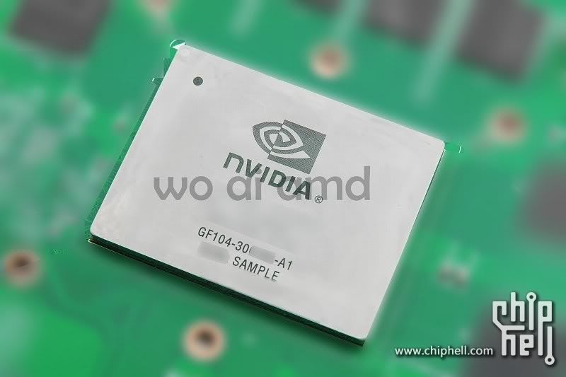
Rumour has it that the GTX 460 is crippled and there will be a GF104-based GTX 468 with full 384 cuda cores, 64 TMUs, and (presumably) 32 ROPs/256-bit/1GB.

www.enet.com.cn

Performance should obviously end up above GTX 465 level (higher clocks, more cores & TMUs) and close to or even on par with GTX 470.

Interesting question would be if it has 8 or 16SMs after all.
 
How many possible combinations allowing 336 and 384SPs parts do they have?

4x GPC * 4x SM * 24 SPs = 384 SPs, 2 SMs disabled = 336 SPs
2x GPC * 8x SM * 24 SPs = 384 SPs, 2 SMs disabled = 336 SPs
4x GPC * 2x SM * 48 SPs = 384 SPs, 1 SM disabled = 336 SPs
2x GPC * 4x SM * 48 SPs = 384 SPs, 1 SM disabled = 336 SPs

Other ideas? There are other possible combinations (e.g. 4/8/12), but this is quite unlikely.

Setups are placed per GPC, geometry units are placed per SM. Considering higher core clock, 2 setups (~ 2 GPCs) should be sufficient.

With 16 SMs total, GF104 would have higher geometry performance than GF100 (I expect HW geometry units in GF100 style). That would be quite an overkill, so 8 SMs seems to be likely.

I think the best combination would be the last one...

2x GPC * 4x SM * 48 SPs = 384 SPs, 1 SM disabled = 336 SPs

... but nVidia possibly has many other reasons, which I didn't take into account :)

//edit: The other question are TMUs... 6-8 per SM? 6 TMUs per SM (48 total) would mean same ALU:TEX, while 8 would make more balanced ALU:TEX ratio...

//edit n.2: my wild guess in colors
 
Last edited by a moderator:
Interesting question would be if it has 8 or 16SMs after all.
Good question indeed.
Well, I faintly remember reading somewhere else that it has 4 GPCs, which would make 16 SM more likely.
There are two more reasons why 16 is more likely, in my opinion:

a) it allows for more fine-grained die-harvesting. With 8 SMs, if two of them have some defect no matter how small, Nvidia would have to disable a whopping 96 cuda cores. With 16, if 2 SMs have some defect they need to disable only 48 cores (like they're doing with the GTX 460).

b) from a chip-design point of view, removing 8 cores from each SM sounds easier than adding 16 cores + 4 TMUs.


My guess based on the information and rumors floating around is that GF104 is basically GF100 minus
- 1/4 of the cores per SM
- 1/3 of the ROPs and memory interface
- 1/2 of the L1 cache
- 2/3 of the L2 cache
- some other double-precision related stuff(?)
 
What if the extra MUL is used again (maybe more efficiently) and Nvidia simply decided to count each SFU as 4 "cores" ?

I haven't been briefed yet, so it's pure speculation ;)
 
TKK: On the other hand, 4/4/24 die would be likely bigger than 2/4/48. Wouldn't it make yields worse?

Tridam: Interesting idea :)
 
What if the extra MUL is used again (maybe more efficiently) and Nvidia simply decided to count each SFU as 4 "cores" ?

I haven't been briefed yet, so it's pure speculation ;)

So not only changing the layout of the SMs but also redesigning the shader core back to MUL, ala G80/92/200?
That isn't impossible but high unlikely IMO.
 
Last edited by a moderator:
Think about it the other way, GF104 -> GF100 rather than GF100 -> GF104.

GT200 -> GF104 : Nvidia double the number of units per SM (16-way FMA + 4 SFUs), it also requires a dual scheduler. They would count these 4 SFUs/ 16 MULs as 8 "cores" to match the other "cores" flops ratio.

Now think about this possible GF104 architecture tweaked to produce a GF100 nicely fit for Tesla market. We can imagine that they extended the main SIMD (16 cores) to support DP and that the second SIMD came relatively cheap because of that. They would then focus on this second SIMD with GF100 rather than trying to extract some MULs from the SFUs. That wouldn't mean they're out of the underlying architecture however.

Again just a theory in the middle of others. Just wrote about it because this one had not been discussed yet.
 
In this case, 4 GPCs seems to be more likely. What about the per-SM geometry unit? Do you expect same approach as in GF100, or emulation via SPs?
 
Damien asked a few questions to ATI and NVIDIA's partners: http://www.behardware.com/news/lire/15-06-2010/

Ouch that's going to be a really crappy situation for Nvidia's partners if it doesn't offer a compensation package when it launches GF104. Assuming GF104 is as good as people are speculating.

Heck even without a GF104 launch it sounds like many partners are basically taking a loss on GTX 470 chips if it is true that they are downgrading them in house to GTX 465 in an attempt to move them and at least not take a total loss.

Regards,
SB
 
Again just a theory in the middle of others. Just wrote about it because this one had not been discussed yet.
An interesting theory nevertheless. I was also thinking "what if" - Nvidia had chosen to develop their GF10x-GPUs not strictly on a one-size-fits-all SM base, but gone the painful way for high-end/HPC parts and stayed rather conservative with their mainstream cards.

Two points spoke against it until recently:
- their focus on mobile parts getting more and more important for developers who supposedly want to take their whole environment with them. But that has been evaporized with GTX480M based on GF100 (which i thought was highly unlikely, but hey!).
- Cost. Pure and simple. After the economic crisis of 2008/2009 I thought they'd rather go on a short budget especially with GF100 apparently being a quite costly development on all fronts. But maybe it was already too late to change plans.

So, is GF104 really what they called a bad idea at the GF100 launch: GT200 with DX11 bolted on? Or does it sport the whole distributed concept of GF100 with some economizations not so important for the gaming market? I wish I'd knew. :)
 
Ouch that's going to be a really crappy situation for Nvidia's partners if it doesn't offer a compensation package when it launches GF104. Assuming GF104 is as good as people are speculating.

Heck even without a GF104 launch it sounds like many partners are basically taking a loss on GTX 470 chips if it is true that they are downgrading them in house to GTX 465 in an attempt to move them and at least not take a total loss.

Regards,
SB
Er, what? Why would nVidia partners be selling any parts if they were taking losses on them?
 
The problem with exposing the MUL is that there's no issue port or decode logic for that now. It would require an increase of the batch size from 32 to probably 64 (think of how the VS had a batch size of 16 on G80). Basically what they've done in GF100 is move slightly more towards CISC and integrate the interpolation request into other instructions (or something equivalent).

It's possible that the reason why they moved to 48 ALUs is that they aren't as batshit insane as I am and realized a multiple-of-2 (i.e. 6) number of TMUs per block wouldn't be efficient enough (or just wouldn't work) so that it's much better to increase both ALU and TMU count from 32 to 48 and 4 to 8 in order to increase the ratio. Then presumably at least one lower-end derivative might keep the 8 TMUs but go back to 32 ALUs. This kind of flexibility would also hint at a theoretical ability to scale down to 4 TMUs/16 ALUs.

Of course this leaves open the question of the number of SFUs/interpolators on GF104. Sharing the same number of units between three schedulers rather than two wouldn't be impossible, but 6 SFUs wouldn't seemingly work unless batch size became a multiple of 6. Which leads us to the very small possibility that the batch size changes from 32 to 48, with all the implications to the previous 'dual scheduler' claims, but that would be very surprising. Given the greater number of TMUs, I think overall the most likely theory is they're sharing twice as many units between 3 schedulers but it's hard to say.

And that's before we even start considering what Tegra3's G80/GF100-inspired CUDA-capable GPU looks like. Better not start thinking about that or we risk total nervous system breakdown.
 
It's possible that the reason why they moved to 48 ALUs is that they aren't as batshit insane as I am and realized a multiple-of-2 (i.e. 6) number of TMUs per block wouldn't be efficient enough (or just wouldn't work) so that it's much better to increase both ALU and TMU count from 32 to 48 and 4 to 8 in order to increase the ratio.
Re-stating the perfectly obvious: That would also greatly benefit the ratio of units doing the heavy lifting against the more auxiliary type of logic.
 
Er, what? Why would nVidia partners be selling any parts if they were taking losses on them?

Just going by the ariticle where it mentions that some OEM's have said they are downgrading their paid for 470 chips into lower priced 465 equivalent chips through the BIOS. The hope being that rather than not moving them at all, they can at least move their inventory.

This is also the reason for which some decided to transform, via a different bios, some Geforce GTX 470s into GeForce GTX 465s, taking on all the costs of the operation themselves as they have paid NVIDIA the price of the GeForce GTX 470 (of the card or just the GPU) and NVIDIA haven’t put any compensation system into place.

So it'll depend on what the price difference is between a GTX 470 chip and a GTX 465 chip as well the price difference of the fully assembled cards. If the profit margin from that is small enough that it's completely eaten by administration and maintenance costs of the company then it could well still be considered taking a loss.

Regards,
SB
 
131559sppfaq4xjxax4162.jpg
 
Back
Top