Nvidia Ampere Discussion [2020-05-14]

Sony is installing a cluster of NVIDIA DGX A100 systems linked on an NVIDIA Mellanox InfiniBand network.
Sony’s engineers are packing machine-learning smarts into products from its Xperia smartphones, its entertainment robot, aibo, and a portfolio of imaging components for everything from professional and consumer cameras to factory automation and satellites. It’s even using AI to build the next generation of advanced imaging chips.

https://blogs.nvidia.com/blog/2021/...582&linkId=100000040843726#cid=_so-twit_en-us
 
NVIDIA Nsight Perf SDK v2021.1 Now Available | NVIDIA Developer Blog
July 6, 2021
The Nsight Perf SDK v2021.1 public release is now available for download.

New features include:
  • Simplified APIs to measure GPU performance within your application, and generate HTML performance reports .
  • Lower-level range profiling APIs, with utility libraries providing ease-of-use.
  • All of the above, usable in D3D11, D3D12, OpenGL, and Vulkan.
  • Samples illustrating usage in 3D, Compute, and Ray Tracing.
New: Ray Tracing Samples

Below is a screenshot of Microsoft’s Real Time Denoised Ambient Occlusion sample, containing Nsight Perf SDK instrumentation. Each render pass or phase of execution has been annotated to take a measurement.
U_eCpiNfgXb3Yt9Jdmv5BvBRZ_lEveq6ycvZ49Au1S9sxB18RUi9axJR9WS2LYh5gzEgoYEYJF6M3i-tIiIbL72BIOCnjjDOYb2h6LOb1imJCdGCRkYZ3AhY7-MjAL-yaLoI8O_2


WytPXbTP77BTGWqykXnuAyi1iGdBsVS3hdUdf4tYozhMj63Gq3iMfTwzMe2orM9jWYCAyWad8vCDbT3cAi4uCqBME7sn9O-NwfOYOqQQ0I9aNF70KeoMtCHEdRp2mq6rYzuEJfRJ
 
Last edited:
NVIDIA® Nsight™ Graphics 2021.5 is released
November 10, 2021

Feature Enhancements:
  • Nsight Graphics & Nsight Aftermath now provide full support for Windows 11
  • NVIDIA NGX is now supported for Linux (in addition to Windows). For more details on NVIDIA NGX, see NVIDIA NGX Technology - AI for Visual Applications
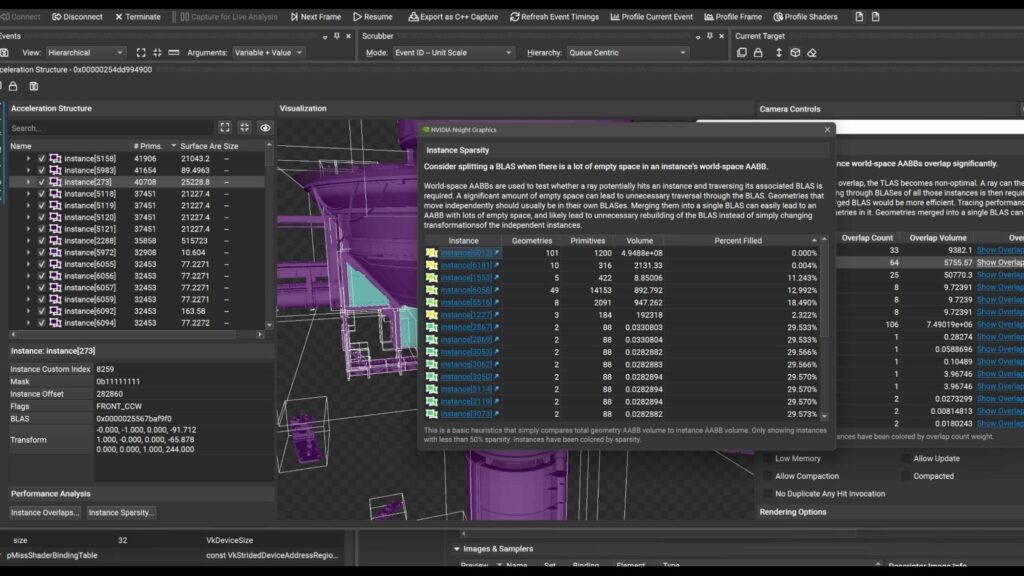
  • Added acceleration structure analysis to the acceleration structure viewer
    • The viewer now offers the ability to see instances that are excessively overlapping, following the best practices for NVIDIA RTX Ray Tracing.
    • See Best Practices: Using NVIDIA RTX Ray Tracing
Improvements:
  • Added an API for providing project parameters to the Nsight Graphics SDK injection API.
  • Added a file-based hierarchical sorting mode to the shader profiler.
    • This allows users to see all of the shaders originating from a particular file.
Additional Changes:
  • Support for graphics debugging and profiling of x86 (32-bit) applications will be removed in a future release. We will continue to support x86 (32-bit) launchers (e.g., Steam, Origin) that start x64 (64-bit) applications.
Known Issues:
  • When profiling ray tracing shaders using the Shader Profiler on a system with the R495 series driver, there is a known issue where samples may not be attributed. These samples will be classified as 'Unattributed'. This issue will be addressed in a future driver release.
  • After generating a trace of Quake II RTX in GPU Trace and clicking Analyze, the host may crash if you repeatedly click and cancel the Aggregate option. If you encounter this crash, please try clearing your app data as a workaround by going to the Help menu in Nsight Graphics and clicking on "Reset Application Data…"
  • Windows 11: Nsight Graphics may show incorrect Exception Summary status in the Reset Channel field of the Aftermath Dump Info tab for Vulkan applications. In addition, Reset Channel may show "3D" instead of "Compute."
image2-3-1024x576.jpg
Nsight Graphics Documentation (nvidia.com)
Download Center | NVIDIA Developer
 
Speaking of RT. Nvidias "Best Practices" mention "Use triangle geometries when possible. Hardware excels in performing ray-triangle intersections. Ray-box intersections are accelerated too, but you get the most out of the hardware when tracing against triangle geometries."

I was under the impression, that Nvidia as well as AMD could perform 4 Box intersections or 1 Triangle intersection per Unit. Has anyone seen more documentation on Ampere (and possibly Turing) in this matter?

Nvidia has never shared the number of box or triangle intersections per clock in shipping products. If I recall correctly their patents referred to compressing 8 boxes into a single cache line so that may be a hint.

"In one embodiment, the TTU may include four traversal units to test up to eight child nodes for intersection with the ray in parallel."

https://patents.google.com/patent/US9582607B2/en
 
Last edited:
Speaking of RT. Nvidias "Best Practices" mention "Use triangle geometries when possible. Hardware excels in performing ray-triangle intersections. Ray-box intersections are accelerated too, but you get the most out of the hardware when tracing against triangle geometries."

I was under the impression, that Nvidia as well as AMD could perform 4 Box intersections or 1 Triangle intersection per Unit. Has anyone seen more documentation on Ampere (and possibly Turing) in this matter?
Ampere's triangle intersection rate is twice that of Turing's isn't it?

The page was written before Ampere came along, August 2020.

Is Ray-box used primarily (solely?) for procedural geometry?
 
Poor wording when you have to make sure that developers do understand exactly what the DOs and DON'Ts for Raytracing are?
 
Strange chart. Why are they starting with 780 and not 680? And with Pascal there was a 600mm^2 die with P100 which hasnt more cuda cores but a better architectur and HBM.
 
Strange chart. Why are they starting with 780 and not 680? And with Pascal there was a 600mm^2 die with P100 which hasnt more cuda cores but a better architectur and HBM.
680 is GK104 whereas 780 Ti is GK100/110 ("full" Kepler) and the 680 is the same as the 770 for reference (8 SMX), P100 isn't a consumer product like V100, A100 and H100 aren't consumer products so they're not mentioned
 
GK110 was ready for the Titan supercomputer in 2012. And the number of cuda cores depends on the amount of transistors nVidia want to spend. TU102 was bigger than P100 and P100 has every graphics function as gaming Pascal.
 

NVIDIA makes new A800 for chinese market, since their A100 and H100 were among the GPUs caught in latest round of sanctions in the trade war.
By the looks of it A800 is A100 permanently limited to max 400 GB/s GPU to GPU bandwidth
 
Back
Top