More hits to the heart for the 4 PE's CPU fans (CELL)

london-boy said:
It's not part of Cell. This was answered already, i think it had to do with testing and stuff. Obviously there is a lot of testing to be done at this stage, maybe that's the reason these early wafers have those extra circuits.

testing after packaging, and not on wafer, i mean
 
version said:
london-boy said:
It's not part of Cell. This was answered already, i think it had to do with testing and stuff. Obviously there is a lot of testing to be done at this stage, maybe that's the reason these early wafers have those extra circuits.

testing after packaging, and not on wafer, i mean

Well then go back to one of the 4 million Cell threads and look for the answer to the same question. It wasn't even 2 weeks ago. It's in the thread with the first pic of Cell.
 
london-boy said:
version said:
london-boy said:
It's not part of Cell. This was answered already, i think it had to do with testing and stuff. Obviously there is a lot of testing to be done at this stage, maybe that's the reason these early wafers have those extra circuits.

testing after packaging, and not on wafer, i mean

Well then go back to one of the 4 million Cell threads and look for the answer to the same question. It wasn't even 2 weeks ago. It's in the thread with the first pic of Cell.

:) , remember , was TEST, but dont think
 
version said:
london-boy said:
version said:
london-boy said:
It's not part of Cell. This was answered already, i think it had to do with testing and stuff. Obviously there is a lot of testing to be done at this stage, maybe that's the reason these early wafers have those extra circuits.

testing after packaging, and not on wafer, i mean

Well then go back to one of the 4 million Cell threads and look for the answer to the same question. It wasn't even 2 weeks ago. It's in the thread with the first pic of Cell.

:) , remember , was TEST, but dont think

+1
 
wafer.JPG


http://www.beyond3d.com/forum/viewtopic.php?p=458854#458854
 
Jaws said:
^^^ Hey, I'm not an expert on wafers but that's an awfull lot of wafer for testing, no?

It's like.. the first Cell chips that have been produced in... EVER. So i guess it's justified.
But i'm beginning to understand version's question. I think he's trying to say, in his very broken english, that there is one circuity bit for each pair of Cell (if you notice). So i think he's thinking they're testing how 2 chips work at a time, fuelling rumours of a double Cell configuration for PS3. I say, let's wait and see. :D
 
Theres space between each Cell and "the other Chip". Why would they do such a thing if its not for being able to seperate them.
To get a Dual Setup Sony would still need to wire the connections, so they could aswell place 2 seperate Cell-Dies beneath each other AND have higher yields (not having to throw away a 2 Cell-Package if one is defect).

Assuming a Dual-setup because of that wafer is nonsense, not that there coldnt be a Dual-setup, but that picture aint giving arguments for or against it.
 
london-boy said:
Jaws said:
^^^ Hey, I'm not an expert on wafers but that's an awfull lot of wafer for testing, no?

It's like.. the first Cell chips that have been produced in... EVER. So i guess it's justified.
But i'm beginning to understand version's question. I think he's trying to say, in his very broken english, that there is one circuity bit for each pair of Cell (if you notice). So i think he's thinking they're testing how 2 chips work at a time, fuelling rumours of a double Cell configuration for PS3. I say, let's wait and see. :D

yeah, i learning engilsh from processor manuals , sorry :)
 
ibmpowerpc.JPG


Another PowerPC wafer...so I take it wafers have these test strips and then for mass production, they are removed for higher yields because they don't seem to be in any other wafer images, right?
 
Which side of the chip has the FlexIO interface? Isn't that on the side with the SPEs? Isn't that the opposite side of that circuit? I can't tell how the chip is oriented, but that's what it looks like to me. Looks like that circuit is on the side with the PPE rather than the SPEs, so it'll be connecting to the memory interface. PEACE.
 
Is it confirmed fact or just a rumor that the area is used for testing ?
Wouldnt it be more likely that the testing circuitry is required in much lower quantities and being factured seperate from the Cell-Wavers - I mean how the hell do the know the testing circuitry itself is good (it has not exactly a insignificant size) ?

Prolly a Chip they will need in a fixed ratio to the manufactured Cells, Cell-Workstation-Northbridge for example( assuming a 2 Cell setup, with alot DDR-RAM through the NB ).
 
zidane1strife said:
O/T semi-related question.

I forgot, why do they make the wafers round instead of square?

From cpiasminc of PSINext.com:

Wafers are round for a couple of reasons. One, you have to grow a giant pure silicon crystalline ingot (or boule). The growth process is done by hanging a seed crystal into a vat of molten silicon, rotating it, and drawing it out slowly. This is repeated several times until you have a desired size. The process is actually pretty similar to how one makes candles.

The boule is machined down to a true cylinder to make handling and a lot easier. Typically, there's also a slight flattening down one side as a handling reference. Among other things, the slicing and polishing process follows, and in general, the ability to evenly polish the boule and the wafers is a lot better when the shape doesn't have any corners.

The other thing is that because of the linear velocity differences as the boule is grown, the crystalline structure eventually starts to weaken as you get further outward in radius. Depending on the angular velocity, there may be a real point where the crystals are too small to be of use. Anyway, that means that no matter what shape you cut the boule down to before slicing and polishing, you can't avoid the fact that images printed towards the outer parts of the wafer are more likely to have defects anyway, so in the end, a circle shape is still equally efficient.

-Rich
 
zidane1strife said:
O/T semi-related question.

I forgot, why do they make the wafers round instead of square?

Quality is best in the middle and lower the further you go to the edge, so the Chips on the edges of a square would be the worst. (I think its because the layers are applied by rotating the wafer and droping the liquid in the center)
 
kaigai002.jpg


kaigai005.jpg


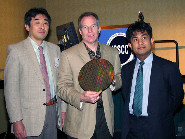
I wouldn't expect more than one CELL but those three STI guys look suspect, especially the one on the left! :)
 
Back
Top