D
Deleted member 86764
Guest
Its a Schrödinger cache!
We've opened the box, observed, and the cat is still both dead and alive.
Its a Schrödinger cache!
I think you may have accidentally used 'IF' (Infinity Fabric) instead of 'IC' (Infinity Cache). Infinity cache is the big GPU L3, Infinity Fabric is an interconnect between various components used on both AMD GPUs and CPUs e.g. connecting the two CCXs on a Zen 2 chiplet, or connecting one chip on a multi-chip-module to another.
If you're talking about Infinity Cache, then I'd agree with everything you're saying.
There are an awful lot of acronyms out there. And if you dig into one you normally find out it's made up of of several more. It's acronyms all the way down ....
I think you mean Infinity Cache. Infinity Fabric is something else and is present in more or less every AMD SoC.
Cache scrubbers and coherency engine ?

Locuza has released a twitter thread on his interpretation of those recently released high quality PS5 die shots.
28 tweets in the thread, this is just the first (the "128-bit FPU on CPU" is from an old tweet, don't get excited!)
Pretty much the same conclusions as from earlier shots ... but now with amazing photos! Worth a couple of minutes if you're interested in that sort of thing.
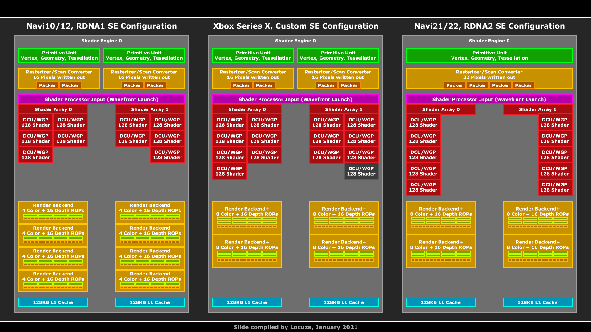
Reminded me of the different render back end in PS5 (RDNA 1 like) and XS (RDNA 2 like). Mulling over a couple of thoughts on that front. I think they could explain one or two things we're seen ... maybe.
PS5 seems to have twice the depth ROPs, and redundant units to boot. Big additional silicon cost vs XSX, and you lose a (potentially) useful RDNA 2 feature. But I think there could be cases - particularly edge cases - where it nets the PS5 a not insignificant advantage. I'll try and think of an example to show what I'm getting at, and where we might see something like it.
Anyway....
PlayStation 5 is especially challenging because the CPU supports 256-bit native instructions that consume a lot of power.
Huh? Xbox features match RDNA2 perfectly, while PS5 and RDNA1 lacks mesh shader capabilities (even if the changes required weren't massive, they were there)- Both Xbox and PS5 have "RDNA 1.5" primitive Unit / rasterizer structure (well RDNA1 actually), not RDNA2.
His (and others) analysis of both APUs showed that:
- PS5 CPU has not (really) a cutdown FPU, allegedly only a few exotic instructions missing but the AVX 256 native instructions should be there. It's not like Cerny didn't make a very precise statement about PS5 supporting AVX 256 native instructions. And Cerny does not talk in riddles or PR talks.
- Xbox Seires X has heavily cutdown ROPs (about half size of PS5 ROPs, PS5 has double Z/stencil ROPs) which could explain plenty of "weird", "unexplainable" framerate drops in many games from launch to now (the last one being little nightmare 2, almost all those games with DRS using different engines).
- Both Xbox and PS5 have "RDNA 1.5" primitive Unit / rasterizer structure (well RDNA1 actually), not RDNA2.
Huh? What exactly is XSX lacking compared to Navi2x? Other than one extra layer of cache which is architecturally irrelevant.Neither is as advanced as the latest AMD products, and we shouldn't get too held up on '1' vs '2' (not saying you personally are!).
Huh? What exactly is XSX lacking compared to Navi2x? Other than one extra layer of cache which is architecturally irrelevant.
You can't really read details like that from highly stylized artist pieces vs actual die shots. Even if there is a difference it could just be a layout thing with exact same functionality to fit the SoC better.In terms of features it's bang on (as far as we can tell), but the front end is structured differently to the block diagrams for PC RDNA 2 parts that released later. So it's probably older.
Truth is that GPUs are modular and in constant development. Modules are ready at different times. Consoles don't have to fit in exactly with PC product roadmaps, and vice versa.
As I said, PC components aren't necessarily the be all and end all for none PC components that exist on a different part of the (branched) roadmap.
You can't really read details like that from highly stylized artist pieces vs actual die shots. Even if there is a difference it could just be a layout thing with exact same functionality to fit the SoC better.
What makes you think that? I mean seriously, we have heavily stylized representations by artist, not dieshots for Navi2x.The differences in the front end seem architectural rather than layout IMO. Don't know how significant those changes are tho...
What makes you think that? I mean seriously, we have heavily stylized representations by artist, not dieshots for Navi2x.
I haven't heard of missing 256bit instructions. What Sony+AMD apparently did was just use high-density transistor libraries instead of high performance ones. Heat density when running 256bit FP instructions @ iso clocks should be considerably greater compared to PC/Series Zen2 APus, but it seems those are pretty rare in gaming workloads so even it pushes the CPU clocks down (like Cerny suggested) it should result in a negligible performance difference.- PS5 CPU has not (really) a cutdown FPU, allegedly only a few exotic instructions missing but the AVX 256 native instructions should be there.
They also can have high heat density thanks to liquid metal cooling.I haven't heard of missing 256bit instructions. What Sony+AMD apparently did was just use high-density transistor libraries instead of high performance ones. Heat density when running 256bit FP instructions @ iso clocks should be considerably greater compared to PC/Series Zen2 APus, but it seems those are pretty rare in gaming workloads so even it pushes the CPU clocks down (like Cerny suggested) it should result in a negligible performance difference.
Perhaps another interesting question is why Microsoft opted out of these area savings, considering the rising costs of high end nodes. They do need to use the Series X SoC on Azure servers, but is that the case with the Series S?
Perhaps another interesting question is why Microsoft opted out of these area savings, considering the rising costs of high end nodes. They do need to use the Series X SoC on Azure servers, but is that the case with the Series S?