AMD: Southern Islands (7*** series) Speculation/ Rumour Thread

Say you're a manager, your architects come to you with two designs, and you have to pick one...

I'm not a manager at an IHV, I'm just a guy who likes to talk about GPUs on the internet :)

In what way is it even useful information, beyond geeky curiosity?

Well that's sorta my point. Most of what we discuss here is just due to geeky curiosity! Stuff like die size and manufacturing cost is mostly irrelevant to us. I am not disagreeing with you that IHV's need to care about the bottom line. I'm just saying that those things aren't very interesting or useful to a discussion on "why" one architecture is faster/better/more efficient than another.
 
So I think something with quite a bit less CUs (but same amount of "other stuff" including ROPs, geometry units) might indeed be slightly better balanced for games. Even the loss of bandwidth might not be that bad (I'm not quite sure how much area this saves, maybe significant if internal busses also can be more narrow etc.).

The 7950 should help shed some light on that. I think the rumours so far mention that only CU's and clocks will get the axe, similiar to the 6970/6950.

In that particular comparison the 6970 is about 12% faster from 10% higher clocks, 10% more bandwidth and 20% more flops so the extra SIMDs are contributing something.
 
I'm not a manager at an IHV, I'm just a guy who likes to talk about GPUs on the internet :)


Well that's sorta my point. Most of what we discuss here is just due to geeky curiosity! Stuff like die size and manufacturing cost is mostly irrelevant to us. I am not disagreeing with you that IHV's need to care about the bottom line. I'm just saying that those things aren't very interesting or useful to a discussion on "why" one architecture is faster/better/more efficient than another.

But faster/better/more efficient has no parameter for gameperf/flops...that does not make an arch any of those three things.

You can only measure performance against die size/cost, and power usage/heat as a limiting parameter, it's literally the only truly relevant efficiency metric.
 
Sorry, you can't prove me wrong with random unsubstantiated claims. At TPU the 7970 is only 70% faster than the 5870 @ 2560x1600 for over twice the transistor count. It's only 38% faster than the 6970 for 65% more transistors. It just gets worse at lower resolutions. Where exactly was I proven wrong? :)

Only 70%?? Ok...

You drew a parallel saying that 7970 is paying a "per transistor" performance price for moving to compute that "Nvidia already paid" That's what I've proved wrong. How are you not following along here, or are you being deliberately obtuse? It's pretty simple. Heck this is just a completely random thing I spotted while googling about GK104, GTX 285 (1.4b) had 71% the performance of GTX 480 (3 b) http://tpucdn.com/reviews/NVIDIA/GeForce_GTX_480_Fermi/images/perfrel_1920.gif. Your theory is shot to hell by now multiple times over just in a couple random examples.

You compared to Caymen, I was pointing out Caymen was a nice improvement on 5870 without moving to compute. Compare SI to 5870 and most of the "per transistor cost" disappears, so it's arguably not "moving to compute" that did the "damage". I dont think any GPU generation gets 100% scaling per transistor these days BTW. I think 70% is close enough. Not counting driver gains, moving to newer games=more performance, etc. It's possible/likely I think you'd agree, that we could get a HD8000 revision that comes close to doubling Caymen for the same transistors as SI. Just as Caymen was a nice improvement on 5870 at the same transistor count.


Where are your numbers to back that up? AMD graphics division still isn't making money. Just look at their statements.

Link? I know little about AMD's financials, except that they've been break even/slightly profitable lately as a whole. I'm just assuming the GPU div is on the helpful side of that ledger. Even so, as you yourself admit, there could be a million factors going on there. The bottom line is as far as we know smaller dies are cheaper, period. Why must you skirt around this issue to the point of all but implying it isn't true?


Meaningful to who? Die size is a rather mundane topic. Yes it's relevant to manufacturing cost but does it provide any insight into architectural details? You're free of course to pretend those questions dont exist while staring blankly at die sizes but it wont make the questions go away.

Too me this all seems like "Nvidia loses here so I dont want to talk about it, shame on you guys for talking about some boring thing that we shouldn't care about harumph". How is die size less relevant than any other details we discuss? It's more so.


How has that worked out for you in the past?

Fine, great, usually. I could be wrong but AMD GPU's seem to age a little better, going back to the likes of X1950XT. (knock on my 4890, still runs BF3 mostly ultra campaign at 30 FPS). It's typically no huge thing I'll admit.


The die size argument is simply sticking your head in the sand. Just looking at the die sizes of say the 580 vs 5870 won't tell you very much about anything.

No, it's looking at a key cost parameter.


Die sizes don't matter at all to me as a customer. I'm not sure how you can start talking about architectural efficiency without first understanding the architectures you're discussing ;)

I admit I dont understand GPU "architecture" very well. But it's easy to compare die sizes and performance.
 
GDS is not really a cache, per se. It's not even a standard memory construct in any cross-vendor API, and acts much like the LDS, but for global synchronization (hence the name) and it's not intended to cache the access to the global memory. This is where the L2 comes to play here.
I guess the GDS has some useful applications, as it can be manipulated on a kernel level, but I'm not really sure what in the presence of a coherent L2. Certainly not for bandwidth amplification or data stream-out between pipeline stages.

GDS acts like a driver managed cache for graphics. One big advantage for this design is predictable performance and no hitting the crossbar for sharing data across pipeline stages.
 
Only 70%?? Ok...

You drew a parallel saying that 7970 is paying a "per transistor" performance price for moving to compute that "Nvidia already paid" That's what I've proved wrong. How are you not following along here, or are you being deliberately obtuse? It's pretty simple. Heck this is just a completely random thing I spotted while googling about GK104, GTX 285 (1.4b) had 71% the performance of GTX 480 (3 b) http://tpucdn.com/reviews/NVIDIA/GeForce_GTX_480_Fermi/images/perfrel_1920.gif. Your theory is shot to hell by now multiple times over just in a couple random examples.

2560 is going be a problem for the 1GB ram of 5870. @1920 the gains from 5870 to 7970 and from GTX 285 to GTX 480 are fairly similar, which supports his notion that nVidia paid the compute penalty with Fermi already and that AMD is now paying it. That comparison is unfair anyway with AMD having a refresh in the middle, whereas with nVidia the starting point GTX 285 was the refresh and 480 had quite a bit of problems getting its potential out.

You compared to Caymen, I was pointing out Caymen was a nice improvement on 5870 without moving to compute. Compare SI to 5870 and most of the "per transistor cost" disappears, so it's arguably not "moving to compute" that did the "damage". I dont think any GPU generation gets 100% scaling per transistor these days BTW. I think 70% is close enough. Not counting driver gains, moving to newer games=more performance, etc. It's possible/likely I think you'd agree, that we could get a HD8000 revision that comes close to doubling Caymen for the same transistors as SI. Just as Caymen was a nice improvement on 5870 at the same transistor count.

Expect the Cayman had 22.5% more transistors and slightly higher clocks than the 5870. I think it's a pipe dream to expect a 8xxx revision to double Cayman performance with only 4.3B transistors. That would require over 2X scaling of transistors, which you seemed to think is unlikely. Cayman had 2.64B transistors.

Link? I know little about AMD's financials, except that they've been break even/slightly profitable lately as a whole. I'm just assuming the GPU div is on the helpful side of that ledger. Even so, as you yourself admit, there could be a million factors going on there. The bottom line is as far as we know smaller dies are cheaper, period. Why must you skirt around this issue to the point of all but implying it isn't true?

http://ir.amd.com/phoenix.zhtml?c=74093&p=quarterlyearnings

You can check the financial tables from there. Graphics have done ok lately, but is quite small compared to their CPU business in size and profit. Although The APU chips are counted in the CPU business despite containing GPUs. For nVidia the vast majority of revenue comes from GPUs, but you are right that the GPU-business does not look too healthy from looking at their numbers, although the latest year was profitable. Their profits come from the Quadro and Tesla lines of products. This is interesting...

Too me this all seems like "Nvidia loses here so I dont want to talk about it, shame on you guys for talking about some boring thing that we shouldn't care about harumph". How is die size less relevant than any other details we discuss? It's more so.

I don't have much else to say to this except I like big silicon :) Performance/size is good but performance alone is far better. Performance/watt is important, but within reason.
 
You drew a parallel saying that 7970 is paying a "per transistor" performance price for moving to compute that "Nvidia already paid" That's what I've proved wrong. How are you not following along here, or are you being deliberately obtuse? It's pretty simple. Heck this is just a completely random thing I spotted while googling about GK104, GTX 285 (1.4b) had 71% the performance of GTX 480 (3 b) http://tpucdn.com/reviews/NVIDIA/GeForce_GTX_480_Fermi/images/perfrel_1920.gif. Your theory is shot to hell by now multiple times over just in a couple random examples.

I hope you see the folly in using a salvage part in a perf/transistor analysis. You know you can't prove somebody wrong by saying "I proved you wrong" right? :D

You compared to Caymen, I was pointing out Caymen was a nice improvement on 5870 without moving to compute. Compare SI to 5870 and most of the "per transistor cost" disappears, so it's arguably not "moving to compute" that did the "damage".

Cayman is more compute focused than Cypress, that was the whole point of moving to VLIW4.

I dont think any GPU generation gets 100% scaling per transistor these days BTW. I think 70% is close enough.

This is how past architectures have scaled per 100% more transistors. All numbers are based on TPU or computerbase launch reviews at 2560x1600. We discussed Cypress' poor scaling to death on these forums. But as you can see there have been transitions that brought 95%+ scaling.

4890->5870: 40%
5870->6970: 95%
6970->7970: 62%

7900->8800: 95%
8800->280: 70%
285->580: 59%


Link? I know little about AMD's financials, except that they've been break even/slightly profitable lately as a whole. I'm just assuming the GPU div is on the helpful side of that ledger. Even so, as you yourself admit, there could be a million factors going on there. The bottom line is as far as we know smaller dies are cheaper, period. Why must you skirt around this issue to the point of all but implying it isn't true?

The link is AMD's website. I'm not implying anything. Of course smaller dies are cheaper, I'm just rebutting your point that smaller dies have done wonders for AMD. I'm not even arguing that point - I'm just stating a simple thing. In response to AlphaWolf's question about perf/mm I'm saying that things will be closer this time around since AMD has now also invested more transistor budget into compute and geometry albeit in a more balanced way than Fermi did.

Too me this all seems like "Nvidia loses here so I dont want to talk about it, shame on you guys for talking about some boring thing that we shouldn't care about harumph". How is die size less relevant than any other details we discuss? It's more so.

So you're going through all this to defend GCN? I'm not attacking the architecture, just stating facts. nVidia has been "losing" the perf/mm battle for years and we've been discussing die sizes for years. My point is that die sizes alone tell you nothing about the underlying architecture and why it performs the way it does. This isn't some new revelation :)

Fine, great, usually. I could be wrong but AMD GPU's seem to age a little better, going back to the likes of X1950XT. (knock on my 4890, still runs BF3 mostly ultra campaign at 30 FPS). It's typically no huge thing I'll admit.

It'll be an interesting thing to investigate but most reviewers dont review old enough hardware nowadays to provide the info we need.
 
36579eea-e1e0-4134-a209-89a10c785965.jpg


nom nom nom :)
http://forums.overclockers.co.uk/showpost.php?p=20902040&postcount=34
 
I'm not a manager at an IHV, I'm just a guy who likes to talk about GPUs on the internet :)

Well that's sorta my point. Most of what we discuss here is just due to geeky curiosity! Stuff like die size and manufacturing cost is mostly irrelevant to us. I am not disagreeing with you that IHV's need to care about the bottom line. I'm just saying that those things aren't very interesting or useful to a discussion on "why" one architecture is faster/better/more efficient than another.

But don't you think that an engineering term like efficiency should be defined using engineering criteria?
 
But don't you think that an engineering term like efficiency should be defined using engineering criteria?

The definition of efficiency is work_rate/resource_usage. It doesn't dictate what resource to use. It can be time, money, energy, die size or theoretical maximums.

e.g http://top500.org/list/2011/11/100 - you can define efficiency there using either Rmax/Rpeak or Rmax/Power depending on what you're trying to evaluate.

Don't get me wrong, I'm not trying to convince you or anyone to care why the 7970 has 2.4x the texturing capacity of a 580. If you choose to ignore that and look only at die sizes that's your perogative :)
 
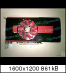
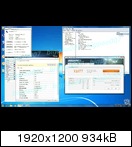
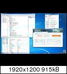
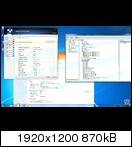
GPU clock 1000MHz
Memory Clock 1125MHz 128 bit
Performance ~6850 -5%
2GB

Is that stock or overclocked?

The definition of efficiency is work_rate/resource_usage. It doesn't dictate what resource to use. It can be time, money, energy, die size or theoretical maximums.

e.g http://top500.org/list/2011/11/100 - you can define efficiency there using either Rmax/Rpeak or Rmax/Power depending on what you're trying to evaluate.

Don't get me wrong, I'm not trying to convince you or anyone to care why the 7970 has 2.4x the texturing capacity of a 580. If you choose to ignore that and look only at die sizes that's your perogative :)

I care because it's interesting, but I don't see how it should in any way make one architecture better than another. I mean you could push perf/flops very high by going full scalar with OoO, a huge re-order window, and 16-way SMT, but what would that get you apart from humongous power draw, cost, and very low absolute performance because you'd never have enough room to put enough execution units on your die?
 
Fudo claims different numbers for 7770/7750.

http://www.fudzilla.com/graphics/item/25363-radeon-hd-7770-brings-28nm-for-$149

"The Radeon HD 7770 is based on the Cape Verde XT chip and it should end up clocked at 900MHz. It has 896 stream processors as well as 56 texture units and 16 ROPs. The memory is clocked at 1375MHz (5.5GHz GDDR5 effective). The runner up is HD 7750 based on Cape Verde PRO, works at 900MHz has 832shaders, 52 TMUs and 16 ROPs. The memory works at 5.0GHz bringing the total possible bandwidth to 80 GB/s for its 1GB of memory. This one will sell for $10 less, or $139."

I care because it's interesting, but I don't see how it should in any way make one architecture better than another. I mean you could push perf/flops very high by going full scalar with OoO, a huge re-order window, and 16-way SMT, but what would that get you apart from humongous power draw, cost, and very low absolute performance because you'd never have enough room to put enough execution units on your die?

It doesn't make one architecture better than another but you can't even come close to drawing that conclusion without understanding relative strengths and weaknesses. There was an obvious difference in priorities for Fermi and Cypress/Cayman so each architecture's strength was apparent. That changes now as Southern Islands is much more balanced and is better at almost everything. That will make for a more straightforward comparison to Kepler.
 
Back
Top