You can see three sets of replicated PHY at the bottom center and next to the top-right probably-SerDes PHY. Ideally, three links would enable 4-chip MCM of Naples to be fully connected. Then the one of the two huge SerDes PHYs (which look like two blocks of 16 lanes) can be optionally an off-chip SMP link, which would allow 4-chip SKUs to have four for glueless 4S, while 2-chip SKUs to have two to match E5.So has anyone seen an interface at looks remotely like the "GMI" interfaces before? I haven't? I have heard that there have been big improvements for PHY on organic sub strait but i dont remember where i read it.......
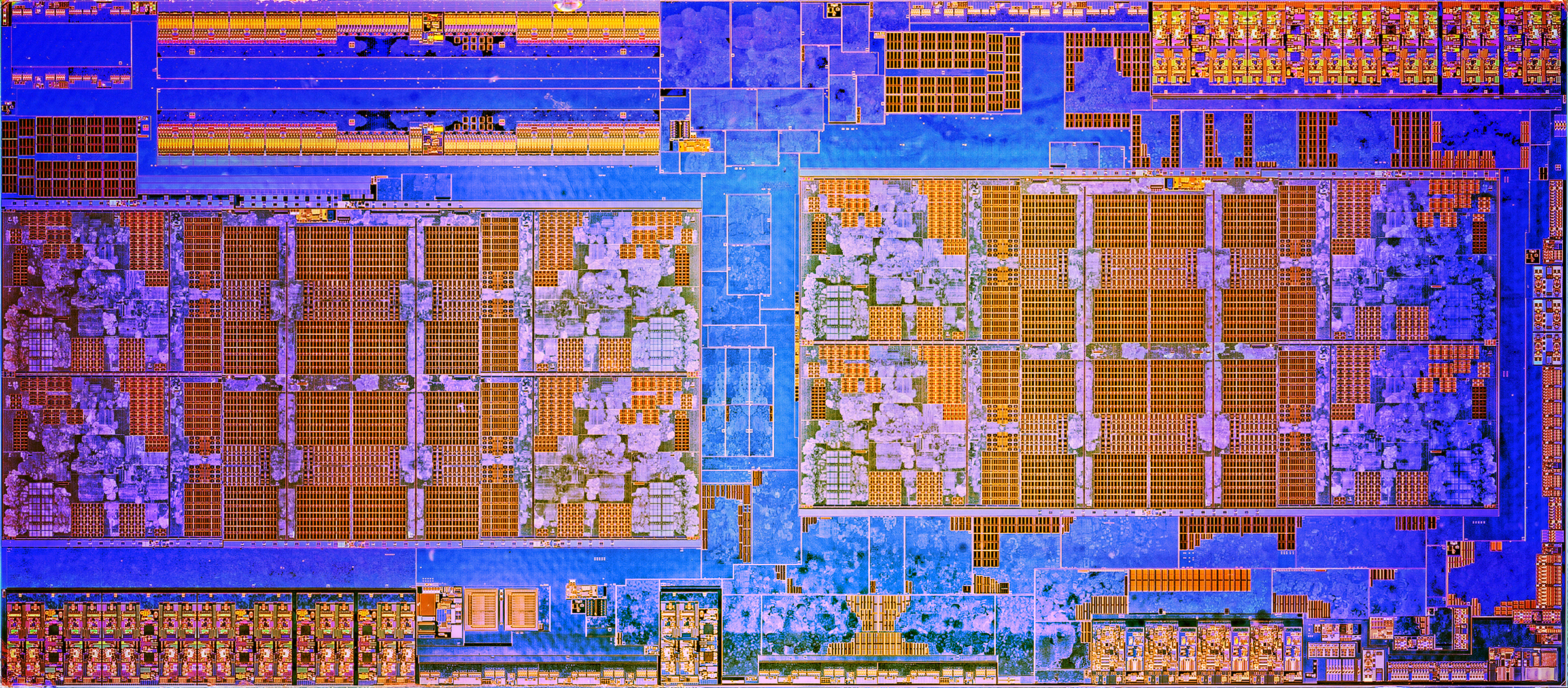
That's said IMO they don't seem to be big enough to be even an on-package >8 Gbps SerDes link to match the bandwidth of three nodes of dual-channel DDR4-2400 or -2667 in one direction. (need 8-10.5 GT/s) I tried to look for die shots with Intel's OPIO but found none. So while perhaps AMD can do some magically-fast-but-miniature on-package I/O (esp. when the off-chip variant seems to be called xGMI instead of just GMI, kudos to VideoCardz), the huge supposedly-PCIe PHY next to them makes it less persuasive.
The top-left huge PHY seems more like the 144-bit DDR PHY, since you can clearly see a pattern of 5-4 blocks which can be seen in Carrizo too.
Last edited:
")