AMD Radeon VII Announcement and Discussion

oh really ? And these tests have what connections to utilizing SSD in the memory pool ? https://www.techpowerup.com/231093/...e-controller-improves-minimum-and-average-fps
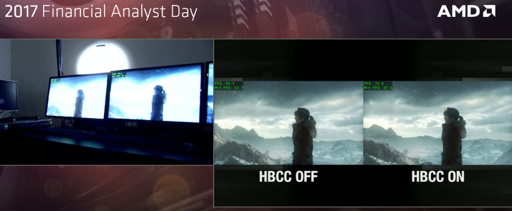
vega-hbcc.jpg

Which applies to the 8GB Vega cards. HBCC is in Radeon VII because it is in Vega 20. HBCC won't be too useful in a gaming card with 16GB of RAM, but it is useful in other configurations and uses for the chips. It could also be VERY useful for consoles, which have a relatively limited memory pool.
 
Whats the point of having HBCC with 16GB of memory pool ?
Utilizing large scratch media like SSDs in the memory pool.

"High Bandwidth Cache Controller" is AMD's marketing term for their crossbar memory/cache/Infinity Fabric controller, so they cannot remove it from the chip.

HBCC uses additional page tables in virtual memory hierarchy to support 49-bit virtual addressing with 4K and 2M page sizes, and to detect and automatically unload unused memory pages from local memory.

This is similar to Direct3D11.2 "tiled resources" (sparse textures) where large data resources are paged in on-demand, which also was a specific implementation of memory paging, but working under explicit developer control over page tables and residency behavior (see Build 2013 session 4-063). This time it's like forced "automatic tiled resources" under explicit control of the video memory manager.

Direct interface to local NVRAM (to avoid PCIe transfers from system memory) is intended for Radeon Pro SSG-class professional products which have 2TB of non-volatile storage.


For me this is the greatest question why? If the silicon or logic was broken they had enough time to test it with Vega 10 and change it in Vega 20.
They say NGG was supposed to work a with existing APIs through driver-level translation, but unspecified performance/optimization issues arose which required explicit support for this combined vertex/domain/geometry stage in high-end APIs like D3D12/Vulkan, and then implementation efforts were stopped for the Vega architecture. That's all we know so far.
 
Last edited:
absolutely nothing with games and thats why they show its benefits in Tomb Raider/Deus EX . LoL


that is my point exactly :) So does it work actually or not ? If yes , why bother then with 16GB of RAM ?

Why are you having so many difficulties understanding this? It was touted as benefiting games on an 8GB card when game had memory requirements that tested that limit. On a 16GB, this probably won't happen. The HBCC has many applications in Vega, so it's going to be in there whether a specific configuration is able to benefit from it or not.
 
Last edited:
absolutely nothing with games and thats why they show its benefits in Tomb Raider/Deus EX . LoL
On a test from a year ago with older Vega cards and simply to showcase the technology in games where you could be VRAM limited. You specifically questioned the technology in relation to 16Gb Vega 20 cards in which I provided other use cases where it was really designed for.
 
On a test from a year ago with older Vega cards and simply to showcase the technology in games where you could be VRAM limited. You specifically questioned the technology in relation to 16Gb Vega 20 cards in which I provided other use cases where it was really designed for.
Don't feed the tro...
 
I suspect the economics depend a lot on the relative volumes of the Radeon Instinct server SKU... If only a small % of chips meet the spec for the Radeon Instinct but many more meet the Radeon VII's specs (not just 60 vs 64 CUs but also power/leakage/etc.) then the cost doesn't really matter, since it's always better than letting those chips go to waste.

That might mean the Radeon VII will be supply limited though, if it's only profitable if the demand for the Radeon Instinct is high enough to only sell "rejects" rather than fully enabled chips... Either way I think it's a very good decision for AMD to release it at $699.
 
If the yields would be abyssal, there probably wouldn't be a Radeon VII. Also why not use 56 CUs variants at all so far, if the yields are that bad? 6.2 TFlop/s DP would still be good for compute-only cards.
 
7nm costs 2 to 3 times the cost of 16/14nm. And that's a fact.

2ywsupl.png


4r9c2e.jpg
BTW - those graphs are theoretically correct but misleading as they don't show how the cost reduces over time. You could find similar graphs for nearly all processes in the last 10-20 years showing a sudden jump in cost for the latest and greatest...

The reality is that new processes are always: 1) very expensive, 2) very defect-prone, 3) very R&D intensive. But after a few years, the cost drops as the equipment is amortised, the yields become really good, and all the tools improve. So those graphs are misleading because they compare mature processes to leading-edge processes.

I think a fair comparison for "normalized cost/yielded mm" would be at "X years after start of risk production" (e.g. 3 years) - if you did that, I suspect you'd see a lot less dramatic increase for 7nm. Of course the *current* cost still matters to decide what process to manufacture a chip on and how competitive a product is; and in that case, the leading-edge process is indeed a lot more expensive in every way. And yes, every process is more expensive than the last, and maybe 7nm will be uniquely much more so even after it matures... but it's probably fine.
 
If the yields would be abyssal, there probably wouldn't be a Radeon VII. Also why not use 56 CUs variants at all so far, if the yields are that bad? 6.2 TFlop/s DP would still be good for compute-only cards.
Agreed but if you're going for even more redundancy, it might make sense to go for 96 ROPs/3072-bit memory bus rather than 128 ROPs/4096-bit (remember it's going to be a significantly higher % of the chip than on 14nm Vega since the memory bus is wider and I/O doesn't scale as much as logic if at all). But at that point the performance might be too low to be competitive and/or attractive, so maybe it'd make the most sense as a special SKU for specific OEMs and/or HPC/AI customers...
 
New bits from PCgamer:
* 1.75GHz boost with 1.85GHz being "a peak achievable" on golden-like samples
* 300W TDP
* a sexy card holder featuring a glued die exists

https://www.pcgamer.com/hands-on-with-the-amd-radeon-vii/


Ok so only anandtech is talking about 128rop/tmu. If it has still 64 (or 60), I'm sure the benchs they used were very bandwidth bound. But in most situations, I don't see a big jump over a well cooled Vega64...

Meh. Where is Navi...
 
yes, I understand it well, Vega is the best architecture in the world. Nothing can match the geniality of RTG engineers. It has no drawbacks at all, every feature is so useful in Vega... HBCC is only for VEGA SGG, Primitive Shaders and NGG path only for NAVI or post NAVI architecture, 128 ROPS which is actually 100% more rasterization power turns into mediocre performance improvements. Yes I know ...

Not everything is the best/worst. Not everyone is for/against. Pointing out where one criticism isn't valid doesn't indicate a belief that all criticisms are invalid.
 
... the cost doesn't really matter, since it's always better than letting those chips go to waste.
Exactly. It’s pointless to talk about profit in this case, and much more meaningful to use gross margin. Radeon VII will increase those for very low additional effort. It’s a no-brainer to release this underwhelming GPU.
 
Have we a confirmation avoir 128 rop / tmu ?
Ok so only anandtech is talking about 128rop/tmu. If it has still 64 (or 60), I'm sure the benchs they used were very bandwidth bound. But in most situations, I don't see a big jump over a well cooled Vega64...
Well Ryan talks about the 128 ROPs in the article itself, not just mentioned in the specs so one would think @Ryan Smith has obtained accurate information.
 
But, If i'm not mistaken, even mi-50/60 don't have that. And I don't see amd making a new gpu. Adding rop is not a small task...
 
Back
Top