
You are using an out of date browser. It may not display this or other websites correctly.
You should upgrade or use an alternative browser.
You should upgrade or use an alternative browser.
AMD: R8xx Speculation
- Thread starter Shtal
- Start date
Believe me, the first thing I did after seeing the BGA was counting of pins to discover, if the GPU isn't 512bit (and no, it isn't).I decided to use my neurons (yes, I still have some) and I discovered something that nobody seems to have noticed.
According to my discovery, the RV870 "could" have a bus of 384 bit !
But it isn't unlikely, that something in RV870 is disabled. Check HD4800 scaling:
HD4830 - GDDR3, 2 SIMDs disabled
HD4850 - GDDR3
HD4870 - GDDR5
HD4890 - GDDR5, new core (+150MHz)
Every part was designed in a way to prevent OC of the weaker model to the performance level of more expensive part. HD4830 is limited by disabled SIMDs, HD4850 is limited by GDDR3 and HD4870 is limited by low OC potential.
HD5850 has GDDR5, so the only way to prevent home-overclockers to get it on HD5870 level was disabling of some SIMDs. HD5890 is on the way, but how could ATi prevent users to overclock HD5870 to the level of more expensive HD5890?
I believe, that the difference will be more significant, than a few MHz. Significantly faster GDDR5? A few more SIMDs (we haven't seen die-shot, everything is possible)? 384bit bus (many pins)? Or even more crazy theory?
")
Btw., as for pins:
R520 - 256 bit - 1025 pins
R600 - 512 bit - 2140 pins
RV670 - 256bit - 1289 pins
RV870 - 256 bit - 1797 pins
NV30 - 128 bit - 12xx pins
G71 - 256 bit - 1275 pins
G80 - 384 bit - 1449 pins
GT200 - 512 bit - 2485 pins
RV770 pin-count would be helpful, I have no idea how many extra pins do the GDDR5 modules require for 256bit bus. Anyway, RV870 has about 250 pins more than G80...
Like ATI already proved us, they can put a 256 bit bus under the RV670, witch have 193,61mm² of surface. However, as everyone knows it, the size of RV870 is 18,25mm x 18,25mm = 333mm², which is enormous compared with the RV670.
Why does the RV870 have 35% more pins ?
RV670 = GDDR3 (69 I/O pins)
RV870 = GDDR5 (62 I/O pins)
The HD 5870 have a 850 MHz frequency, and some customs cards will soon have 900 or 950 MHz frequency.
Then I ask you, what's left for the Radeon HD 5890 ?
Much higher frequency ? Don't think so.
Would it be possible that the RV870 is in fact hiding a weapon of massive destruction ?
If you really want to have a good comparison you should compare it with the RV770 (4870 or 4890) because this GPUs need roughly the same power so the amount of power/grounding pins would be more comparable.
I found only this image:
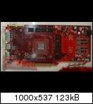
The central part is covered, unfortunately. Visible part has about 1267 pins. If the covered part has the same density of pins, than RV770 has about 1492 pins (200 more than RV670).
So... RV870 has 300 pins more than RV770 (which had about 200 pins more than RV670 to support GDDR5, sideport and higher power consumption).
Errrmmmm...why is there still a discussion of the tech specs of a launched product? Didn't the review sites already said it has 256bit bus? Do you believe there are some kind of hidden surprises? I mean ok speculating before the launch is one thing, but speculating after 100 reviews is another!
Could all this be indicative that there is too much wishful thinking, because people think that ATI underdelivered and they are waiting for some kind of miracle? And no, I am not suggesting that they underdelivered, I am just wondering if people think so (I do have an opinion on the subject, but this is not the point of this post).
Could all this be indicative that there is too much wishful thinking, because people think that ATI underdelivered and they are waiting for some kind of miracle? And no, I am not suggesting that they underdelivered, I am just wondering if people think so (I do have an opinion on the subject, but this is not the point of this post).
For a 4*64-bit interface that would be 4*17 COMM/ADDR wires and 8*44 for the DQ lines, so the overall sum should be 420 pins/balls.I have no idea how many extra pins do the GDDR5 modules require for 256bit bus.
I'm just bookmarking this post for the G300 launch. If the 5870X2 tops the G300 then its a terrible product from XMAN26's perspective.I'm running GTX260 216s in SLi, why should I bother to upgrade to this card?
fellix: 420 pins total for GDDR5 or extra over GDDR3?
Radeon X800 was introduced as a GPU with 12 pipelines. XT part with 16 pipelines wasn't officially mentioned until introduction of 16-pipelined NV40. There isn't any single die-shot of RV870. I wouldn't be surprised by anything.Errrmmmm...why is there still a discussion of the tech specs of a launched product? Didn't the review sites already said it has 256bit bus? Do you believe there are some kind of hidden surprises? I mean ok speculating before the launch is one thing, but speculating after 100 reviews is another!
Could all this be indicative that there is too much wishful thinking, because people think that ATI underdelivered and they are waiting for some kind of miracle? And no, I am not suggesting that they underdelivered, I am just wondering if people think so (I do have an opinion on the subject, but this is not the point of this post).
Total.fellix: 420 pins total for GDDR5 or extra over GDDR3?
G80 -----> 8800 Ultra -> 235W TDP -> GDDR3 (69 I/O pins) -> 384 bit -> 1449 pinsErrrmmmm...why is there still a discussion of the tech specs of a launched product? Didn't the review sites already said it has 256bit bus? Do you believe there are some kind of hidden surprises? I mean ok speculating before the launch is one thing, but speculating after 100 reviews is another!
RV870 --> HD 5870 ---> 188W TDP -> GDDR5 (62 I/O pins) -> 256 bit -> 1737 pins
Why ?!
TOAO_Cyrus
Newcomer
So you guys are saying they intentionally gimped the bus and saved it for a refresh?
We aren't saying anything... just wild speculations
G71 - 287M tr. - 256bit - 1275 pins
RV670 - 666M tr. - 256bit - 1289 pins
That's similar difference in number of transistors, but pinout wasn't affected... Anyway, thaks for GDDR5
You forgot this:
G80 -----> 681M transistors
RV870 --> 2154M transistors
//more grounding
G71 - 287M tr. - 256bit - 1275 pins
RV670 - 666M tr. - 256bit - 1289 pins
That's similar difference in number of transistors, but pinout wasn't affected... Anyway, thaks for GDDR5
So you guys are saying they intentionally gimped the bus and saved it for a refresh?
It's a possibility, a small one, but a possibility nontheless.
RBEs + PCIe + UVD + .... = 306M transistors.The RV740 is 312 million transistors more complex than the RV730. As a result, it has twice the computing capacity (640 ALUs against 320 ALUs) and twice the rasterization performance (16 RBEs against 8 RBEs). On the other hand, the new chip is 130 million transistors simpler than the RV770. Considering that the graphics cores of the Radeon HD 4830 and Radeon HD 4770 have the same configuration (640 ALUs, 32 TMUs, 16 RBEs), we can calculate the theoretical cost of the two disabled SIMD modules of the former. Easy to see, 160 ALUs (32 superscalar processors) and 8 texture processors take 130 million transistors, and one such module takes 65 million transistors. ... As we’ve said above, the RV740 has eight SIMD modules, so the total amount of transistors for the computing and texture resources of the RV740 is 520 million. For the RV770 with its 10 SIMD modules the number is 650 million transistors. Thus, there is 306 million transistors left for each GPU. They are used to implement the rest of the GPU subunits: RBEs with memory controllers, task scheduler, PCIe interface, display controllers, UVD video processor and HDMI audio core.
One SIMD = 65M transistors.
RV870 = RV770x2.
RV770 = 956M transistor -> RV770x2 = 1912M transistors.
RV870 = 2154M transistors.
Difference: 242M
242M is suffisant for 3.7 x SIMD (doh ?) or 2 SIMD (160 ALU and 8 TMUs) + 2 RBEs (16 ROPs) + 2 MC (128 bit bus)
Suffisant number of transistors to implement some "things".
Suffisant number of pins for a 384 bit bus.
Last edited by a moderator:
G80 -----> 8800 Ultra -> 235W TDP -> GDDR3 (69 I/O pins) -> 384 bit -> 1449 pins
RV870 --> HD 5870 ---> 188W TDP -> GDDR5 (62 I/O pins) -> 256 bit -> 1737 pins
Why ?!
Maybe power pad & support for 6 monitors
While your efforts are nice but sorry to burst your bubble that DX11 compliance also has a die-"price". And I think it was Jawed or Arun who earlier had more accurate figures of die spaces wrt SIMDs, TMUs etc.It's a possibility, a small one, but a possibility nontheless.
RBEs + PCIe + UVD + .... = 306M transistors.
One SIMD = 65M transistors.
RV870 = RV770x2.
RV770 = 956M transistor -> RV770x2 = 1912M transistors.
RV870 = 2154M transistors.
Difference: 242M
242M is suffisant for 3.7 x SIMD (doh ?) or 2 SIMD (160 ALU and 8 TMUs) + 2 RBEs (16 ROPs) + 2 MC (128 bit bus)
Suffisant number of transistors to implement some "things".
Suffisant number of pins for a 384 bit bus.
It's a possibility, a small one, but a possibility nontheless.
RBEs + PCIe + UVD + .... = 306M transistors.
One SIMD = 65M transistors.
RV870 = RV770x2.
RV770 = 956M transistor -> RV770x2 = 1912M transistors.
RV870 = 2154M transistors.
Difference: 242M
242M is suffisant for 3.7 x SIMD (doh ?) or 2 SIMD (160 ALU and 8 TMUs) + 2 RBEs (16 ROPs) + 2 MC (128 bit bus)
Suffisant number of transistors to implement some "things".
Suffisant number of pins for a 384 bit bus.
I believe the difference is more. Someone on this forum made a more accurate calculation and found out that there are about 500M transistors more than what they should be in RV870. But it's also true that AMD/ATi said that the scheduler of RV870 would have been twice as complex as RV770 one. It maybe be the transistor cost of DirectX11.
Though, RV730 has about 500M transistor and it has 320 ALUs, 32TMUs, 2 RBEs and 2 MC + other things.
It could be that RV870 has a 384bit MC and also 4 more SIMD. It would be great for the HD5890, but it would get way too close to the performance area of the HD58x0X2s.
Similar threads
- Replies
- 16
- Views
- 3K
- Replies
- 220
- Views
- 88K
- Replies
- 90
- Views
- 13K
- Replies
- 172
- Views
- 19K