Install the app
How to install the app on iOS
Follow along with the video below to see how to install our site as a web app on your home screen.
Note: This feature may not be available in some browsers.
You are using an out of date browser. It may not display this or other websites correctly.
You should upgrade or use an alternative browser.
You should upgrade or use an alternative browser.
AMD: R7xx Speculation
- Thread starter Unknown Soldier
- Start date
- Status
- Not open for further replies.
I say it's crap. It's clearly written by a very "uneducated" person - the R680 certainly does not "rely" on the PLX bridge for communication.
Why? The two gpu are linked through the bridge chip, or not?
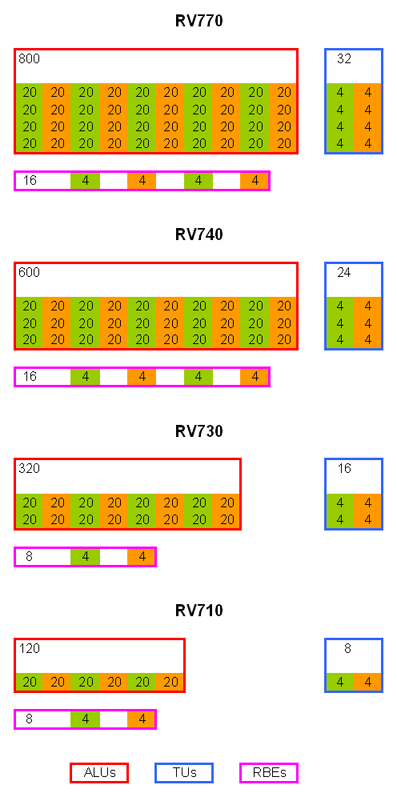
So RV770 will show up with more ALUs than MHz? 
The whole skepticism about 800 ALUs was due to people scoffing that ATI could more than double ALUs, double TMUs, and maintain a die size a notch or two below NV. It still sounds like too tall an order, but I guess it couldn't hurt ATI to surprise us.
To support GDDR5, did they have to mess with their RBEs or with their ring bus? Just trying to figure an extra excuse for them to double Z/clk.
http://forums.vr-zone.com/showthread.php?t=285719
Linked through the memory? Does anyone have an idea of what this could mean?
Yes. See the current discussion thread on this.
The main purpose of the bridge chip is to redistribute the PCIe lanes to the two chips. For communication, there's another interface - the "CF bridge" (which you use to connect two boards in CrossFire; it's routed through the PCB on X2 cards), although some communication goes through the PCIe bus. I wouldn't call that "rely on PLX for communication" though.Why? The two gpu are linked through the bridge chip, or not?
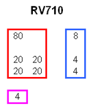
No, certainly not. The games use 4 of the 5 "SPs" on average (there are different shader commands with different "width" and some games generally use "wider" shaders than others). There's no way you could leverage the potential of a 10-way unit with that, hence there'd be no real performance difference between, say, 320 5-way ALUs and 320 10-way ALUs.Had a strange thought last night... how about 80 10-way units instead of 160 5-way ones?
Curious why all the 32 TMU talk... 20 or 40 would seem to make more sense if it is 800 ALUs.
Why? 160 5D ALUs (800 SPs) and 32 TMUs ~ nice 5:1 ALU:TEX ratio... I'm not saying this is real configuration of RV770, but it's not impossible...
leoneazzurro
Regular
I went to bed last night thinking "if it's really 800:32, that's amazing."
I wake up and find it's definitely 800 and extremely likely to be 32 and I'm gobsmacked
I'd already concluded, based upon RV635->RV670 scaling where 60% extra die-space delivers 2-3x performance, that the scalability of this architecture is good - but this is outrageous.
We're looking at ~1.1 billion transistors for RV770?
With that much ALU it seems inevitable that it'll generally be TU:RBE limited. Crysis performance on a single RV770 is going to be an eye-opener because HD3870X2 scales really badly.
Jawed
I think the count, based on the size, is more on a 950 million transistors, give or less 50 million. And I think that each TMU block will be bigger, or, better, to have 2 TMU blocks tied to each sublevel in the SIMD.
Because 160 5D ALUs is either going to be 5 clusters of 32 or 10 clusters of 16. Each cluster will have 8TA and 4TF if it follows R6xx's design.no-X said:Why? 160 5D ALUs (800 SPs) and 32 TMUs ~ nice 5:1 ALU:TEX ratio...
EDIT: Though, 5 clusters of 32 with 8TA and 8TF would make the most sense to me given the die size...
Jawed
Legend
2 TMU blocks like Fellix suggested?:I think the count, based on the size, is more on a 950 million transistors, give or less 50 million. And I think that each TMU block will be bigger, or, better, to have 2 TMU blocks tied to each sublevel in the SIMD.
http://forum.beyond3d.com/showpost.php?p=1129739&postcount=604
Code:
 #0    #1    #2    #3    #4    #5    #7    #8    #9   ||  #0    #1
[ALU] [ALU] [ALU] [ALU] [ALU] [ALU] [ALU] [ALU] [ALU] || [TEX] [TEX]
[ALU] [ALU] [ALU] [ALU] [ALU] [ALU] [ALU] [ALU] [ALU] || [TEX] [TEX]
[ALU] [ALU] [ALU] [ALU] [ALU] [ALU] [ALU] [ALU] [ALU] || [TEX] [TEX]
[ALU] [ALU] [ALU] [ALU] [ALU] [ALU] [ALU] [ALU] [ALU] || [TEX] [TEX]
Jawed
http://forums.vr-zone.com/showthread.php?t=285719
Linked through the memory? Does anyone have an idea of what this could mean?
Wasn't the shader clock rumor discarted?
The main purpose of the bridge chip is to redistribute the PCIe lanes to the two chips. For communication, there's another interface - the "CF bridge" (which you use to connect two boards in CrossFire; it's routed through the PCB on X2 cards), although some communication goes through the PCIe bus. I wouldn't call that "rely on PLX for communication" though.
OK. Thank you for the clear explanation.
So that news is pointless. There will always be the need of a bridge chip with such a configuration... So the real difference should be on how the gpus communicate, if through a CF bridge or through a different kind of connection. If I understood well, so even an Hypertransport connection (I know that is unlikely, just doing an example) will be compatible with the presence of a PLX chip on the PCB?
Wasn't the shader clock rumor discarted?
Yes, Andreas from NordicHardware confirmed the reliability of his source in the XtremeSystems forum.
So maybe the news is crap, but I was trying to better understand the matter... :smile:
Well, speaking theoretically, why not.A.L.M. said:If I understood well, so even an Hypertransport connection (I know that is unlikely, just doing an example) will be compatible with the presence of a PLX chip on the PCB?
leoneazzurro
Regular
2 TMU blocks like Fellix suggested?:
http://forum.beyond3d.com/showpost.php?p=1129739&postcount=604
Code:#0 #1 #2 #3 #4 #5 #7 #8 #9 || #0 #1 [ALU] [ALU] [ALU] [ALU] [ALU] [ALU] [ALU] [ALU] [ALU] || [TEX] [TEX] [ALU] [ALU] [ALU] [ALU] [ALU] [ALU] [ALU] [ALU] [ALU] || [TEX] [TEX] [ALU] [ALU] [ALU] [ALU] [ALU] [ALU] [ALU] [ALU] [ALU] || [TEX] [TEX] [ALU] [ALU] [ALU] [ALU] [ALU] [ALU] [ALU] [ALU] [ALU] || [TEX] [TEX]
Jawed
Yes, but with only 5 SIMDs
[2xALU] [2xALU] [2xALU] [2xALU] [2xALU] || [TEX] [TEX]
[2xALU] [2xALU] [2xALU] [2xALU] [2xALU] || [TEX] [TEX]
[2xALU] [2xALU] [2xALU] [2xALU] [2xALU] || [TEX] [TEX]
[2xALU] [2xALU] [2xALU] [2xALU] [2xALU] || [TEX] [TEX]
[2xALU] [2xALU] [2xALU] [2xALU] [2xALU] || [TEX] [TEX]
where the 2xALU states a group of shader units 2 time sbigger than in the previous scheme.
uhm.. regarding the die size, is it really only 255 - where does that number really come from?
If we look at the photoshopping in post 2602 the calculation is wrong (no squaring of the difference and rv670 is not square), so we get (height, width in pixels):
100/80*101/88 = 1.43 *rv670 = 275mm2
and if I take this image of 4850 and compensate for the perspective distortion I get:
53 (die width)
* 201/186 (distance between parallel lines trough mounting holes at die/pcie measure points)
/ 292 (pcie connector width)
* 89mm (pcie connector width according to wikipedia)
= 17.45mm die width
~ 305mm2 die area
If I do the same (except perspective correction) on this 3850 image I get 211mm2 for rv670, so using this as error correction (maybe the plastic cover isn't included, or is the pcie length wrong?):
305 * 192/210 = 278mm2
Pretty close numbers based on different images/methods
- Status
- Not open for further replies.
Similar threads
- Replies
- 85
- Views
- 17K
- Replies
- 5
- Views
- 4K
- Replies
- 177
- Views
- 42K
D
- Replies
- 220
- Views
- 93K


