NVidia Hopper Speculation, Rumours and Discussion

Nvidia coprocessors can be found in 154 of the TOPP500 supercomputers; only seven of the supercomputers are using AMD Instinct cards.


Good PR. Just try to read between the lines though.
You are totally misleading the article. Supercomputer use a lot of GPUs and CPUs. One small failure could have big impacts on results. (Chaos Theory, butterfly effect) That’s the challenge. I think also Nvidia is facing the same issues. When you have 10.000 GPUs of caus 100 could be dead. That’s 0,1% of all GPUs, so no big deal. So please Stop your Nvidia propaganda.
 
Last edited:

Grace-Hopper evaluation benchmark test results are starting to crop up.
Kicking off our NVIDIA GH200 Grace Hopper benchmarking at Phoronix is an initial look at the 72-core Grace CPU performance with 96GB of HBM3 memory. Here are some initial benchmarks of the Grace CPU performance while the Hopper GPU benchmarks will be coming in a follow-up article.
...
NVIDIA's GH200 combines the 72-core Grace CPU with H100 Tensor Core GPU and support for up to 480GB of LPDDR5 memory and 96GB of HBM3 or 144GB of HBM3e memory. The Grace CPU employs Arm Neoverse-V2 cores with 1MB of L2 cache per core and 117MB of L3 cache.

The other processors featured for this initial GH200 CPU benchmarking included:

- EPYC 8534P
- EPYC 8534PN
- EPYC 9554
- EPYC 9554 2P
- EPYC 9654
- EPYC 9654 2P
- EPYC 9684X
- EPYC 9684X 2P
- EPYC 9754
- EPYC 9754 2P
- Xeon Platinum 8280 2P
- Xeon Platinum 8380
- Xeon Platinum 8380 2P
- Xeon Platinum 8490H
- Xeon Platinum 8490H 2P
- Xeon Platinum 8592+
- Xeon Platinum 8592+ 2P
- Ampere Altra Max M128-30
- GPTshop.ai GH200

Other CPU performance tests ...
The benchmarks shown at the HPC Asia conference last week are perhaps the most detailed we've seen thus far, with the Barcelona and New York researchers each presenting their findings at the conference. Each group tested differently, with the Barcelona benchmarks focusing on Grace's performance relative to Skylake-X's, and the New York tests comparing Grace to a variety of other AMD and Intel CPUs.

 
Last edited:
Paper includes architectural topics as well as H800 benchmarks.

21 Feb 2024
In this research, we propose an extensive benchmarking study focused on the Hopper GPU. The objective is to unveil its microarchitectural intricacies through an examination of the new instruction-set architecture (ISA) of Nvidia GPUs and the utilization of new CUDA APIs. Our approach involves two main aspects. Firstly, we conduct conventional latency and throughput comparison benchmarks across the three most recent GPU architectures, namely Hopper, Ada, and Ampere. Secondly, we delve into a comprehensive discussion and benchmarking of the latest Hopper features, encompassing the Hopper DPX dynamic programming (DP) instruction set, distributed shared memory, and the availability of FP8 tensor cores.
...
This paper delves into memory hierarchy and tensor core performance of the newest three Nvidia GPU architectures using instruction-level benchmarks. We found that the hopper architecture shows advantages in both memory bandwidth and tensor core that are consistent with official claims. It is worth noting that on tensor core, we need to use the latest wgmma instructions to take advantage of all the performance of the fourth generation tensor core. We analyze AI performance across diverse architectures at library and application levels, emphasizing the impact of varied precisions. Experiments show that when the operation scale is relatively large, low-precision data types will show greater advantages. Additionally, we explore key features of the Hopper architecture: DPX, asynchronous data movement, and distributed shared memory. Our research enhances comprehension of the latest architecture’s traits and performance, aiding in optimized algorithm design and application performance.
 
Last edited:
Phew, I was worried there for a second they were doing a lot of the same tests than I've been working on, but there's not much overlap and it's a lot less low-level than what I'm planning to analyse. I haven't looked into Distributed Shared Memory properly yet but I can't make sense of their results, so either they're doing something wrong, or I'm going to have to spend more time than I expected to figure it out...

Also if anyone has anything specific they'd really like tested/analysed on H100 (and AD102/A100 potentially if I have the time), let me know - I'm running dangerously out of time given my intention to publish something before NVIDIA GTC though.
 
March 14, 2024
If we travel back 2 years in time, before the rapid rise in AI, much of the datacenter hardware world was chasing CXL. It was promised as the messiah to bring heterogenous compute, memory pooling, and composable server architectures. Existing players and a whole new host of startups were rushing to integrate CXL into their products, or create new CXL based products such as memory expanders, poolers, and switches. Fast forward to 2023 and early 2024, and many projects have been quietly shelved and many of the hyperscalers and large semiconductor companies have almost entirely pivoted away.
...
Currently, CXL availability is the main issue, as Nvidia GPUs don't support it, and with AMD the technology is limited to the MI300A. While the MI300X can theoretically support CXL in hardware, it is not exposed properly. Availability of CXL IP will improve in the future, but there exist deeper issues than just availability that render CXL irrelevant in the era of accelerated computing.

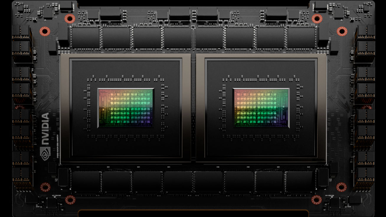
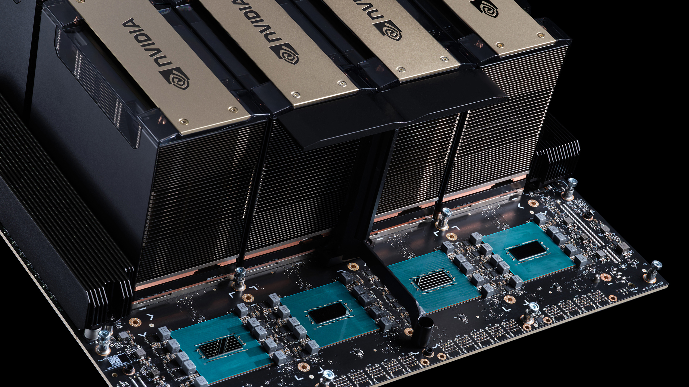
A H100 GPU has 3 IO formats: PCIe, NVlink, and C2C (for connecting to Grace). Nvidia has decided to include only the minimum 16 PCIe lanes, as Nvidia largely prefers the latter NVLink and C2C. Note that server CPUs, such as AMD’s Genoa, go up to 128 lanes of PCIe.

The main reason for this choice is bandwidth. A 16-lane PCIe interface has 64GB/s of bandwidth in each direction. Nvidia’s NVlink brings 450 GB/s bandwidth in each direction to other GPUs, roughly 7x higher. Nvidia’s C2C also brings 450GB/s bandwidth in each direction with the Grace CPU. To be fair, Nvidia dedicates far more beachfront area to NVLink, we so need to include silicon area in that equation; but even so, we estimate that per mm² across a large variety of SOCs, Ethernet-style SerDes such as Nvidia NVLink, Google ICI, etc have 3x more bandwidth per unit of shoreline area.

Therefore, if you are a chip designer in a bandwidth constrained world, you are making your chip roughly 3x worse when you chose to go with PCIe 5.0 instead of 112G Ethernet-style SerDes. This gap remains with next generation GPUs and AI accelerators adopting 224G SerDes, keeping this 3x gap with PCIe 6.0 / CXL 3.0. We are in a pad limited world, and throwing away IO efficiency is an insane tradeoff.

The main scale up and scale out interconnects for AI Clusters will be proprietary protocols such as Nvidia NVlink and Google ICI, or Ethernet and Infiniband. This inferiority is due to intrinsic PCIe SerDes limitations even in scale up formats.
...
Ethernet-style SerDes are much less constrained by stringent PCIe specifications, allowing it to be much faster and have higher bandwidth. As a result, NVlink has higher latency, but this doesn’t matter as much in the AI world of massively parallel workloads, where ~100ns vs ~30ns is not a worthy consideration.

First off, the MI300 AID uses most of its beachfront area for PCIe SerDes instead of Ethernet-style SerDes. While this gives AMD more configurability in terms of IFIS, CXL, and PCIe connectivity, it results in the total IO being about 1/3 that of Ethernet-style SerDes. AMD needs to immediately move off PCIe-style SerDes for their AI accelerator if they want to have any hopes at competing with Nvidia’s B100. We believe they will be for MI400.


TL;DR​

  • A single NVIDIA GH200, enhanced by ZeRO-Inference, effectively handles LLMs up to 176 billion parameters.
  • It significantly improves inference throughput compared to a single NVIDIA H100 or A100 Tensor Core GPU.
  • The superchip’s GPU-CPU 900GB/s bidirectional NVLink Chip-to-Chip (C2C) bandwidth is key to its superior performance.

We first tested the Bloom 176b model with CPU-offload, where the NVIDIA GH200 Grace Hopper Superchip achieved significantly higher throughput compared to H100 and A100 GPUs, showcasing the benefits of its high bandwidth. Specifically, the GH200 produces 4-5x inference throughput of H100, and 9-11x inference throughput of A100, thanks to its significantly higher chip-to-chip bandwidth that removed the communication bottleneck for CPU-offload.

M-K1qOuPbjUB3STyoqzJx9-M5YYpCMc5MrmA-8-y6U2oSD0Z5Gu9fRoLM3aXB-DquHxTAQP4jmPCWJhfcDgR-yc9AJjPIwHBdR1MGtCtaaf1zsCCg2-d8VleYhXbacoBdPJU-2coe1tT


Our second benchmark tested the throughput with/without CPU-offload on the GH200, and saw if CPU-offload can produce overall higher throughput. The figure below shows that when the same batch size is used, CPU-offload inference indeed slightly reduces the throughputs. Nonetheless, CPU-offload also enables running inference with larger batch size (in this case, 32) and produces overall the highest throughput, 1.5x the highest throughput of inference without CPU-offload (using batch size 32, compared to batch size 16, the max without offload).

N8VWlQo7cY7Z0PNICELslI6EQxmlrB0SzhbB4NAavjLHA1-lzLbdvK_ixmih0UJUseSZ2JYLgnsYRrfpNkQLNhtR_VHzLkBK1swP3r_zm4z_UXhjfiWu2eaHQS_XnhS0mfuYZ8r5ttf5
 
Last edited:
Back
Top