"The days of monolithic mega-chips are gone." - Rick Bergman, AMD.
This phrase was the inspiration of my multi-GPU concept.
So, what do you think of it ? Is it viable ?
(Yeah, I know... my photoshopping skill is out of this world.  )
)
With the same two chips (Master & Slaves) AMD can make is entry-level, mid and high-end parts.
HD 54x0 : 1 Master + 1 Slave
(maybe a one-in-all chip is preferable for the low-end )
HD 5670 : 1 Master + 2 Slaves
(with lower clock for the 5650)
HD 5850 : 1 Master + 3 Slaves
HD 5870 : 1 Master + 4 Slaves
And for the HD 5870-X2, I don't know if it's feasible a all.
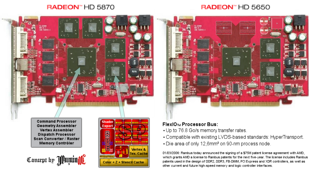
The Master chip will contains all the redundant features (RAMDAC, UVD, PCIe, VIVO, ...) and 4 FlexIO Processor Bus.
Each of the slaves chip will contains SP, TMU, RBE, ..., and some caches.
Only 2 chips to develop and produce -> this can save a lot of time and money.
AMD can upgrade the Master chip (new UVD, new output, ...) without modifying the Slave chip, or other way around.
My concept it is based on some infos that I found here and there:
"01/03/2006: Rambus today announced the signing of a $75M patent license agreement with AMD, which grants AMD a license to Rambus patents for the next five-year. The license includes Rambus patents used in the design of DDR2, DDR3, FB-DIMM, PCI Express and XDR controllers, as well as other current and future high-speed memory and logic controller interfaces." (
LINK)
If AMD paid Rambus $75M
(when they don't have a $ to waste), they must want something from them...
"The FlexIO processor bus can be backward compatible with existing LVDS-based standards, including HyperTransport, SPI-4, and RapidIO, allowing easy integration into next-generation products, while providing a path to higher levels of performance." (
PDF - 711Kb)
Notice the 14-letters word starting with an "H" ? :smile:
"The FlexIO interface is organized into 12 lanes, each lane being a unidirectional 8-bit wide point-to-point path. Five 8-bit wide point-to-point paths are inbound lanes to Cell, while the remaining seven are outbound. This provides a theoretical peak bandwidth of 62.4 GB/s (36.4 GB/s outbound, 26 GB/s inbound) at 2.6 GHz. The FlexIO interface can be clocked independently, typ. at 3.2 GHz. 4 inbound + 4 outbound lanes are supporting memory coherency." (
WIKI)
FlexIO is very fast, is backward compatible with HyperTransport, is support memory coherency, and is a well-proved technology (PS3).
So I think it's the best technoloy for multi-GPU, and maybe AMD is thinking the same way...
Or do you think that Hector wants to throw $75 millions of dollars out of windows ?
I don't know if AMD will implement this kind of multi-GPU with his R800 or R900.
I don't even know if my concept is viable/possible or not.
But it's the way I view it.
Some additional info:
· FlexIO area = 12,6mm² with 90-nm process node:
WIKI.
· Rambus FlexIO bus picture:
PICTURE (
original link)
Some related patents:
·
US Patent 7325086 - Method and system for multiple GPU support
(Issued on January 29, 2008)
·
US Patent 7340557 - Switching method and system for multiple GPU support
(Issued on March 4, 2008)