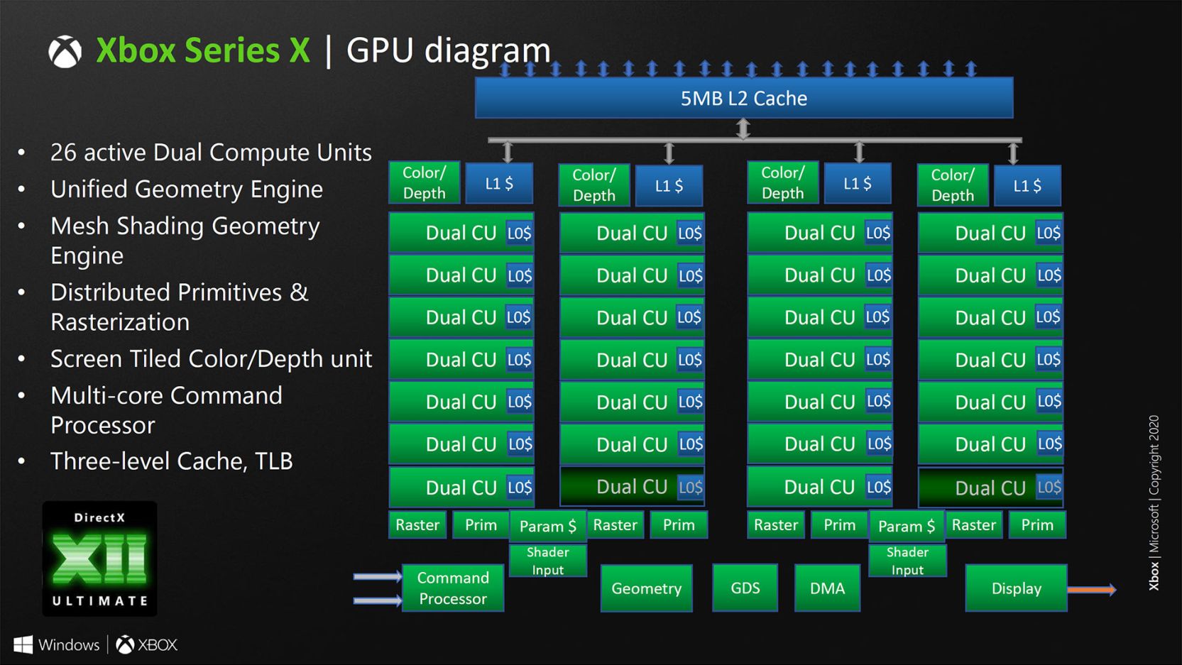
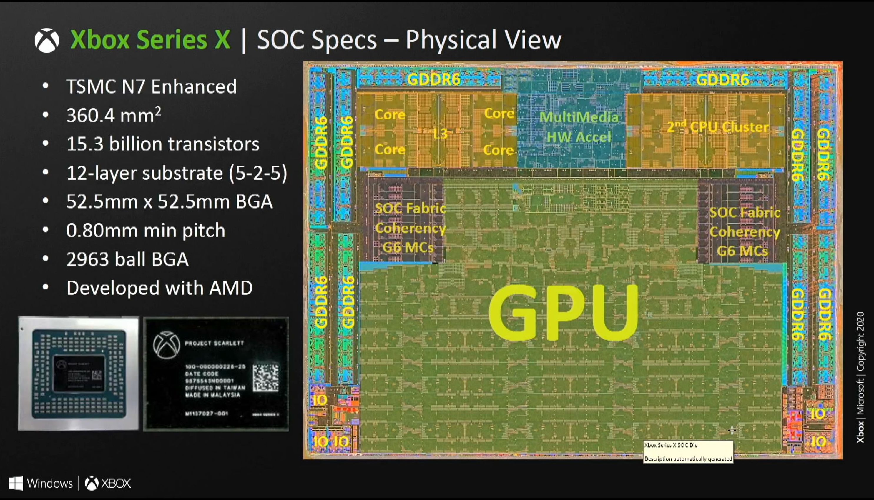
My Theory why AMD packed RT Cores in TMUs.
My theory prior to this being confirmed was that there were two potential areas in the GCN architecture that could be adapted for RT rather than creating a new domain: the shared scalar pipeline with its own memory subsystem, or the texturing path with its own ability to calculate addresses and perform operations on data before passing the filtered result back.
RDNA2 reduced the independence of the scalar path, but that still left the portion of the pipeline related to the texturing units. RT operations have a lot of memory accesses and scheduling, so the texturing path's already existing handling of the vector memory subsystem and its independence from the SIMD hardware would allow for a similar function to be added.
128MB isn't very much all things considered. Intel's old Crystal Well IGP has 128mb of L4 for something like 1/20th the performance. Would be an interesting to see how it works out.
At 32x the size of Navi 10's L2, the old rule of thumb that miss rate scales with the square root of capacity would give a miss rate of ~18% that of the 4MB cache. A more streaming workload may not see as much benefit, but it's also possible that if the size footprint of the cache grew enough it would reach a threshold where there data in-cache could be resident long enough to derive significant reuse.
The area of a GPU L2 and its associated hardware isn't that compact, and even a more dense implementation like Zen2's L3 would give over 100mm2 just for cache.
Bandwidth-wise, it would seem like this cache should provide enough transactions to be equivalent to whatever memory bus it is compensating for, though that would cost density.
Redgamingtech also claims that rdna2 beyond 2.23ghz produces logic problems, supported by someone from Sony on the ps5 apparently.
What logic problems could arise due to high frequencies?
Every chip driven by a clock signal allocates a certain amount of time for each pipeline stage. Signals need to propagate through layers of logic between stages, and there is some minimum time before all signals can be safely assumed to have reached the end of the stage before the next clock cycle. Some parts of the chip tend to take longer compared to others, and if the clock period shrinks enough, some portions of logic can no longer be relied upon to function as expected across the operating range of the chip. Whatever appropriate behavior the chip should have would become prone to failure, which could be seen as data corruption or instability.
Wouldn't cache be helpful in reducing the amount of memory traffic for BVH traversal and thus speed up ray tracing?
It could reduce miss rates off-chip, although depending on how the cache hierarchy is implemented it may not be significantly faster in terms of latency, since GPU cache hierarchies tend to take similar or more time than the actual DRAM access.


