AMD RyZen CPU Architecture for 2017

I'm leery of trying to extrapolate too much from AMD-provided "die shots" given the fuzziness and what AMD has done before when it comes to manipulating pre-launch pictures.
I tried to compare with DDR4 interfaces elsewhere like Haswell E, and some comparisons in MS paint could put the rough area of a single interface+controlling logic around 11mm2, and if we assume the perspective correction and area are accurate for the AMD picture, it's .06 of the image and could put it around 180-200mm2, with huge error bars.

edit: I was using the annotated picture and stupidly forgot to take the heading out.
With that done the range is above/below ~180mm2, still with huge error bars either way.

That might put the core area in that annotated diagram in the ~5mm2 range. In comparison, it seems like a Skylake core in the 6700k might be in the ~8mm2 range. That's including the L2 and a potentially larger vector unit. The "L2" for Zen would be in the 1-1.5mm2 range.
(edit: Correcting for the earlier error puts the core in 4-5mm2 range.)

At least at first glance, the way the core and L2 and L3 areas are annotated seems plausible.
The way the broader wafer shot draws the cuts actually seems off to me. There's more spanning the black line between the left side of a core cluster and the silicon on the right side of the other die, rather than the expanse in the middle.

I'm assuming the bright areas that form the asymmetric grid of the L3 represent parts where data bus lines have to hit higher metal layers, and similarly bright areas in the core areas are related to congested portions of the core like the front end and caches. (edit: interfaces with caches)
The asymmetry of the L3 might come from not needing its full width to route the L3 and coherent interconnect through/over the core complex

As for whether this is an upscaled Jaguar cluster. At least right now, I'd say not quite. Jaguar's LLC was an L2 that was separated from the cores by a big unified interface. I'm not sure this is the case even within a cluster, and the L2s as labeled are tied to the cores.

edit: Since I'm making edits. What would the benefit be in having the DDR4 interface put on both sides of the die? Nobody else seems to have a problem with putting memory on one side and not crowding other connections.
 
Last edited:
There are LinkedIn profiles saying Zen has distributed memory controllers. So each compute unit has something like 4cores l3 1 ddr4 interface and I assume a distributed north bridge.

Edit: I would also assume one gmi interface per northbridge. So a 32 core chip has an 8 stop ring across 4 chips on an interposer.
 
The placement of the DDR4 interfaces is what I have questions about. The supposed GMI interface that would need to link to other sockets, or if older slides were believed, a GPU on the same package.

Is there any CPU or APU that would take a dual-channel interface, split it up onto two sides of the die, and sit the halves right next to an inter-die bus on one side and whatever southbridge IO there is on the other? So far I haven't found anything that doesn't try to keep memory on one side and all that IO on the other.

If this were the basis for the Zeppelin APU concept, that would put some of the DDR4 interfaces in an awkward spot with the GPU that is supposed to hook into the GMI portion.
 
I'm guessing it's mirrored like that to get a internal l3/north bridge interface to face each other. In a choice of optimal off chip wiring or optimal on chip wiring I guess they chose the on chip. Also given that those wires likely just go straight up to bumps/Marco bumps. Does it really matter. A slightly more complicated interposer on a high margin product seems like a fair trade off....
 
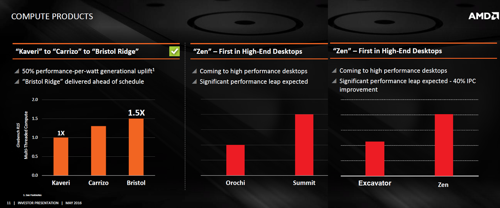
Apparently they updated that slide to IPC
http://dresdenboy.blogspot.co.nz/2016/05/first-amd-summit-ridge-wafer-spotted.html?m=1
Zen%2BPerf.png

Newer version of the slide has the right hand bit with Excavator vs Zen & 40% better IPC specified.
 
That will be a good motivation for Intel to make a 6 or 8 core LGA1151 processor without IGP.
I don't think Intel will compromise on the IGP for their mainstream platform. LGA2011 already serves the many-core market just fine, without the need for cannibalization from the lower end. I would rather see them invest in more robust IGP and L4 cache (eDRAM, HBM), spanning more SKU models. Quad-core with high IPC is good-enough for the time being.
 
I don't think Intel will compromise on the IGP for their mainstream platform. LGA2011 already serves the many-core market just fine, without the need for cannibalization from the lower end. I would rather see them invest in more robust IGP and L4 cache (eDRAM, HBM), spanning more SKU models. Quad-core with high IPC is good-enough for the time being.

The Zen AM4 socket has 1331 pins supporting dual 64 DDR4 DRAM bus.
Apparently that will be sufficient to support the 8 cores without IGP.

If Zen turns out to be the performance monster as it looks like, that will be a very interesting option for many gamers,
at a price point far lower as the LGA2011 equivalents.
 
Since Intel is generally de-emphasizing the classic PC market, the impact from the new AMD product line should be earth-shattering to change the direction of the big blue elephant.
Hell, I think Intel would be just OK for AMD to take a bit of the PC slice, if it only means to keep them more sustainable for a while, for the nominal competition sake.
But even if that happens, the only viable response from Intel would be price adjustments, not platform shifting. And that's exactly what I realistically hope for to happen.
 
Nehalem had 1366 (IIRC) pads for triple DIMM interfaces for just four cores (of course later expanded to 6.) Today's desktop Intel chips have 11xx pads of course for dual DIMMs and PCIe 16x. What does AMD need 1331 pins for if it only has dual DIMM? Does that chip even have PCIe integrated? I see no mention on the die overlay.
 
Nehalem had 1366 (IIRC) pads for triple DIMM interfaces for just four cores (of course later expanded to 6.) Today's desktop Intel chips have 11xx pads of course for dual DIMMs and PCIe 16x. What does AMD need 1331 pins for if it only has dual DIMM? Does that chip even have PCIe integrated? I see no mention on the die overlay.

Power. The pins needed for power and ground goes up as the voltage goes down.
 
Nehalem had 1366 (IIRC) pads for triple DIMM interfaces for just four cores (of course later expanded to 6.) Today's desktop Intel chips have 11xx pads of course for dual DIMMs and PCIe 16x. What does AMD need 1331 pins for if it only has dual DIMM? Does that chip even have PCIe integrated? I see no mention on the die overlay.

LGA1366 pinout:
GksThq1.gif


The uncoloured pins are what's left for functional interfacing (memory, periphery I/O, etc.). Everything else is for power supply provisioning, debug probing and redundancy.
 
Last edited:
I'm guessing it's mirrored like that to get a internal l3/north bridge interface to face each other. In a choice of optimal off chip wiring or optimal on chip wiring I guess they chose the on chip. Also given that those wires likely just go straight up to bumps/Marco bumps. Does it really matter. A slightly more complicated interposer on a high margin product seems like a fair trade off....
The leaked HPC diagram, the need for an inter-socket connection, and rumors of a 32-core MCM hint strongly at it crossing on package and PCB as well.

Unless there's something significant in area or power terms, tweaking a little silicon once when engineering the chip is going to be a minor one-time change versus adding costs off-die. Perhaps there's something that can be gained off-die by spacing things that way?
 
Power. The pins needed for power and ground goes up as the voltage goes down.
Intel desktop sockets have had the same number of pins for many years now despite shrinking silicon geometries. Fewer now than in the beginning, actually. Reportedly, skylake had the integrated voltage regulator from haswell removed, but did not increase pin count in the socket.
 
Nehalem had 1366 (IIRC) pads for triple DIMM interfaces for just four cores (of course later expanded to 6.) Today's desktop Intel chips have 11xx pads of course for dual DIMMs and PCIe 16x. What does AMD need 1331 pins for if it only has dual DIMM? Does that chip even have PCIe integrated? I see no mention on the die overlay.

Maybe 32x PCIe? Or some other amount.
BTW every PC CPU other than AM3+ now integrates PCIe, even AMD ones.

I wonder if they would support registered ddr4? (Intel does with Xeon E5-1620v3 and up, which is kind of a special branded i7)
There are niches of high mem users than can use that.
 
BTW every PC CPU other than AM3+ now integrates PCIe, even AMD ones.
Yeah, which is why I thought it strange with no mention on the notated die shot. Of course, that's a very blurry image, it could simply be that it's difficult to correctly identify the interface. :)
 
So Lisa Su showed a heat-spreadered Zen at Computex, ran a video of the logo (running on a Zen PC apparently), confirmed 8 core 16 thread, expects sampling to big customers in next few weeks.
Not exactly groundbreaking news though.
 
So Lisa Su showed a heat-spreadered Zen at Computex, ran a video of the logo (running on a Zen PC apparently), confirmed 8 core 16 thread, expects sampling to big customers in next few weeks.
Not exactly groundbreaking news though.

It suggests Zen is on time. For a brand new CPU architecture from AMD, that's kind of a big deal. Has it ever happened?
 
It suggests Zen is on time. For a brand new CPU architecture from AMD, that's kind of a big deal. Has it ever happened?

Athlon 64?

Regardless, it depends on what you mean with "on time".
Zen may be "on time", but it's not like AMD set themselves up for any speed record on putting a new architecture out there.
Zen started its development in 2012.
Between 2012 and late 2016, ARM will have transitioned from Cortex A9 to Cortex A15, then mid-gen transition Cortex A12/A17, then major transition to ARMv8 with Cortex A57, then Cortex A72, then mid-gen transition Cortex A73.. and that's only in the high-end.
Intel did two "Tick-Tocks" and a half, practically 6 different CPU cores from Sandybridge to Kaby Lake.

Considering the rather small upgrades that the Bulldozer family got throughout the years, it's a bit hard to believe their blunt workforce was focused on that architecture.
At least Sledgehammer was delayed. Intel was having its own issues at the time, so that wasn't as problematic.

Zen coming out in 2016-2017 is just about right if it is a new high-end core. 4-5 years is the rule of thumb for a project of that magnitude, without tacking on delays. Looking at the release dates of other companies shows more about the throughput of their pipeline than its length.
Development of the next generation is ongoing during the lifetime of one or more predecessors.
AMD has a problem with throughput due to limited resources, poor retention, and divided attention between multiple product types and its semicustom division. The period when it didn't have a formal CEO was also rumored to have come with a spending freeze that effectively injected a "bubble" of sorts into the development pipeline as well, which was not seen until much later.
 
Back
Top