snc
Veteran
From official manual sony didnt write what rdna they using so it can be stil rdna1 with some custom adjustments, just sayingSo now we have added PS5 Pro doesn't do hardware RDNA3 dual issue to the FUD pile.
From official manual sony didnt write what rdna they using so it can be stil rdna1 with some custom adjustments, just sayingSo now we have added PS5 Pro doesn't do hardware RDNA3 dual issue to the FUD pile.
He must do this from now on. Every unboxing. The packaging must be destroyed to upset the audience.Maybe Rich should have first Lot some incence and doused holy water over the PS5Pro think cardboard Box. Now that would be true respect befitting a sacred professional machine.
In ever more elaborately destructive ways!He must do this from now on. Every unboxing. The packaging must be destroyed to upset the audience.
Maybe Rich should have first Lot some incence and doused holy water over the PS5Pro think cardboard Box. Now that would be true respect befitting a sacred professional machine.
WRT Dual Issue - things change, maybe the OG Version of PS5Pro was going to be dual issue, but they got rid of it for die space?
It helps compute Performance a Bit in Games, but not exactly a whole bunch in a way they might have seen as necessary for their bottom line.
Have Chad warden make a cameo to make it timeless. PS quintuple professional.Yes please. Now if you could all redo that video dressed in gowns while Gregorian chants play, it would be appreciated.
If Sony claim 33.4TFLOPs now, they will have a lot of marketing problems when announce PS6.
Marketing power fell foul after the PS360 era. One can count all sorts of Flops and OPs to generate bigger numbers. I wouldn't read too much into it, in contrast to not advertising features such as ML frame generation.Doubt it's for that, and a potentional PS6 should be much more than 33TF. It is all about AI and ray tracing in the future, marketing wise. It's already now.
If you got a 33TF product you're not going to market just half of that, it doesn't make much sense.
Nothing's confirmed. The only official information I think we have is the leaked tech docs and Mark Cerny's engineering statement and now what's included in the PS5. We also have this new software engineer statement. These sources aren't consistent. Cerny said, "Custom hardware for Machine Learning and an AI Library." That would naturally lead to general purpose ML functionality in hardware with software to drive upscaling. Now we have Bezrati, Principle Engine Programmer at Insomniac, calling it "an actual custom silicon AI upscaler (and antialiasing)...that frees up a lot of the GPU" which can only really mean a functional block dedicated to the job. Then we have the leak that Globby pointed to with numbers that match the theory of ML residing in the Compute and TF counts that match RDNA3 theories but statements like 'full custom design'.Again could it be that the GPU is based on the 4 year old RDNA2 CU's? It would be roughly comparable in raw power to a vanilla RX6800 which in turn is close to a 7700XT which is 35TF? That wouldn't be too bad, mid range performance untill RDNA4 and Nvidias next GPU's. Or is it confirmed that its RDNA3+?
From what we know of Series Consoles and PS5 as per earlier break down of the products, both are customized away from RDNA2 to be able to support backwards compatibility, there was a series of tweets going around looking at very nuanced differences between RDNA2, and GCN1.1 etc. Even the current generation consoles have some sort of connection to GCN1.1 in some aspects for these reasons. I believe around the ROPs mainly, there was also something about wave submissions as well, but for some reason my memory isn't recalling just right.Doubt it's for that, and a potentional PS6 should be much more than 33TF. It is all about AI and ray tracing in the future, marketing wise. It's already now.
If you got a 33TF product you're not going to market just half of that, it doesn't make much sense.
Again could it be that the GPU is based on the 4 year old RDNA2 CU's? It would be roughly comparable in raw power to a vanilla RX6800 which in turn is close to a 7700XT which is 35TF? That wouldn't be too bad, mid range performance untill RDNA4 and Nvidias next GPU's. Or is it confirmed that its RDNA3+?
it sure can, 16.7tf 32bit ->33.4tf 32bit dual-issue -> 66.8tf 16bit dual-issue67 TF 16 bit precision in those leaks struggles to reconcile with Sony's new official 16.7 TF figure. Where does that 67 TF number come from? Not even dual-issue can account for that.
I think I may have found it, though I could be wrong on my interpretation here.I think the most likely scenario is no dual issue. It still seems unlikely there are dedicated cores for AI math which leave the GPU free to do other work. The existing upgrades certainly don't support that IMO.
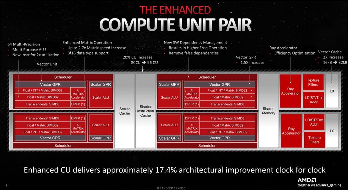
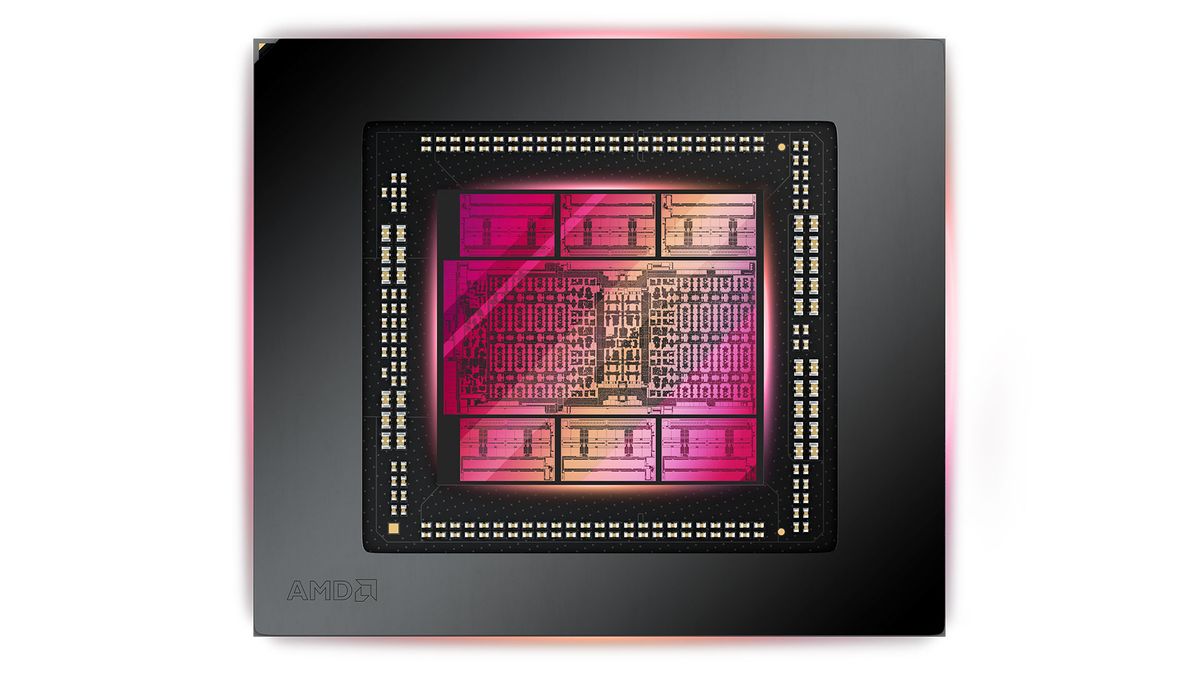
A cursory look at the above might not look that different from RDNA 2, but then notice that the first block for the scheduler and Vector GPRs (general purpose registers) says "Float / INT / Matrix SIMD32" followed by a second block that says "Float / Matrix SIMD32." That second block is new for RDNA 3, and it basically means double the floating point throughput.
You can choose to look at things in one of two ways: Either each CU now has 128 Stream Processors (SPs, or GPU shaders), and you get 12,288 total shader ALUs (Arithmetic Logic Units), or you can view it as 64 "full" SPs that just happen to have double the FP32 throughput compared to the previous generation RDNA 2 CUs.
This is sort of funny because some places are saying that Navi 31 has 6,144 shaders, and others are saying 12,288 shaders, so I specifically asked AMD's Mike Mantor — the Chief GPU Architect and the main guy behind the RDNA 3 design — whether it was 6,144 or 12,288. He pulled out a calculator, punched in some numbers, and said, "Yeah, it should be 12,288." And yet, in some ways, it's not.
AMD's own specifications say 6,144 SPs and 96 CUs for the 7900 XTX, and 84 CUs with 5,376 SPs for the 7900 XT, so AMD is taking the approach of using the lower number. However, raw FP32 compute (and matrix compute) has doubled. Personally, it makes more sense to me to call it 128 SPs per CU rather than 64, and the overall design looks similar to Nvidia's Ampere and Ada Lovelace architectures. Those now have 128 FP32 CUDA cores per Streaming Multiprocessor (SM), but also 64 INT32 units. But whatever the case, AMD isn't using the larger numbers.
Your deduction is very reasonable and makes a lot of sense, particularly in the confines of a console. I hope we get an exact answer at some point in the future. @Bondrewd has said dedicated, tensor style cores aren't coming anytime soon in any consumer facing tech. I don't know if he legitimately has insider info though.I think I may have found it, though I could be wrong on my interpretation here.

AMD Radeon RDNA 3 Architecture Overview: Efficiency Is King
AMD has revealed more details about its newly launched RDNA 3 architecture including refinements to the compute unit and how it links chipletshothardware.com
RDNA 3 Architecture Overview:

Note the AI Matrix Accelerator is inside the Vector GPR.
Note the following blocks under the Vector GPR:
Float / Int / Matrix SIMD 32
Float / Matrix SIMD 32
SIMD8
DPFP - Dual Precision Floating Point AKA FP64 unit
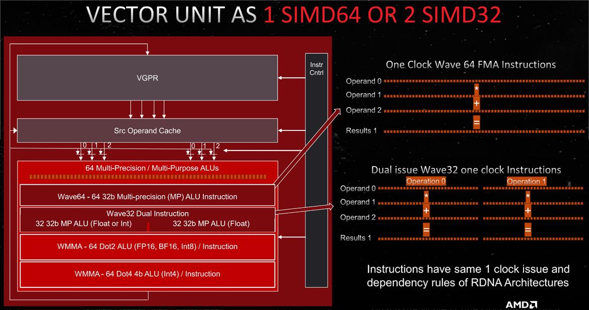
Lets break down the Vector GPR to get more details (from AMD)

Here we see the:
FP64 Unit up top
We see the 2 SIMD32 Units
We See this Transcendantal Int8 WMMA
And now we have this Int4 WMMA but missing is the 'AI Matrix Accelerator' from above.
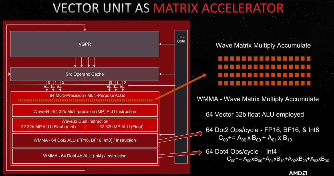
So lets look at the next picture

First off - the Title of the slide is VPGR as a Matrix Accelerator.
So what we're seeing here is the bottom 2 blocks now being used in conjunction with that FP64 to do Matrix acceleration calculations.
So now we know what AMD is labeling as an AI Matrix Accelerator Unit.
So if they can leverage FP64 unit to do this and instead of dual issue FP32 that is doing it. It's clear the math is the same.
1FP64 breaks down into 8x int8 * 2 for sparsity
Which brings us back to 16x TOPs.
16.7 * 16 = 267 TOPs
They may do a little more here with RDNA 4, but I think this is it here. The dual Issue is not required for them to achieve the 300 TOPs as the AI Matrix accelerator uses the FP64 ALUs and they can save money by removing the other FP32 unit. Though this isn't proof that there isn't dual issue FP32. Just that, it appears dual issue FP32 is not necessary for the WMMA to do their work.
I dunno, I also feel like I could be reading this block completely wrong. And that what is being described as FP64 is just another mode for the SIMD32 to operate in.
If this is the case, I can't see how they would get away without the 2nd SIMD32 unit. They would definitely have both, it would support Dual Issue FP32, they just aren't marketing it.
edit: Using this article from Tom's Hardware:

AMD RDNA 3 GPU Architecture Deep Dive: The Ryzen Moment for GPUs
Swimming with the next generation GPUswww.tomshardware.com
So there is precedent here for using the lower number for SPs. I think if Sony is following this labelling format, they are using the lower number.
From what I remember with RDNA3 dual issue isn't usable with rapid packed math (which is their mechanism for fp32->2xfp16).it sure can, 16.7tf 32bit ->33.4tf 32bit dual-issue -> 66.8tf 16bit dual-issue

Very cool benchmarks! From this site we have:From what I remember with RDNA3 dual issue isn't usable with rapid packed math (which is their mechanism for fp32->2xfp16).
If you look at microbenches for RDNA2 vs. 3 for example they have comparable fp16 throughput once you account for FPUs and clocks.

Microbenchmarking AMD’s RDNA 3 Graphics Architecture
Editor’s Note (6/14/2023): We have a new article that reevaluates the cache latency of Navi 31, so please refer to that article for some new latency data.chipsandcheese.com
Now, lets talk about that 123TFLOP FP16 number that AMD claims. While this is technically correct, there are significant limitations on this number. Looking at the RDNA3 ISA documentation, there is only one VOPD instruction that can dual issue packed FP16 instructions along with another that can work with packed BF16 numbers.
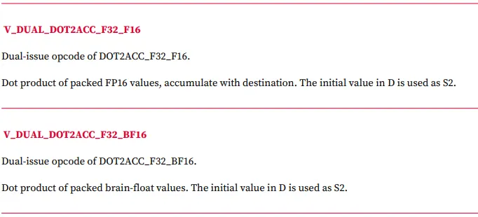
This means that the headline 123TF FP16 number will only be seen in very limited scenarios, mainly in AI and ML workloads although gaming has started to use FP16 more often.
Why enable the quality mode settings in the performance mode if it's going to perform like that?
I don't believe it's anywhere near an RTX 4070 in this game.
They should keep settings of performance mode but boost internal res. In their article about keeping internal res they mention they didnt see benefit in boosting res but clearly is visible difference between pssr quality and perf mode, not sure whats with remedy devs eyesWhy enable the quality mode settings in the performance mode if it's going to perform like that?
It seems 864p is too much for pssr and 30fps mode is still the way to play in AW2 on pro.
