AMD: Southern Islands (7*** series) Speculation/ Rumour Thread

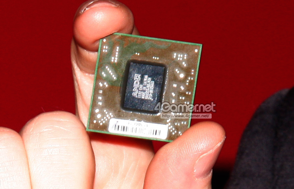
It's not rotated within the package, so it has more in common with Juniper, than say Cypress.

What's the average size of a shirt button?
If it's 1cm, eyeballing the pic makes me think it's somewhat larger than Juniper. Maybe 210-230 mm2?

It's too blurry and I didn't work too hard to get a good measure.
 
It's not rotated within the package, so it has more in common with Juniper, than say Cypress.
Then again, it could be GCN architecture too so any previous chip references would be null.
(And even it's VLIW, it's VLIW4 for sure, not 5, so nothing much common with Cypress nor Juniper)
 
I was talking is about the packaging, not the architecture on the chip.
The trend for the big chips is that they are rotated in the package, while the smaller ones are not.
Perhaps it is due to bus width, but that also trends with die size.

edit: RV770 was not rotated, so it could be because of die size.
 
What's the average size of a shirt button?
If it's 1cm, eyeballing the pic makes me think it's somewhat larger than Juniper. Maybe 210-230 mm2?

It's too blurry and I didn't work too hard to get a good measure.
I just did a quick estimate under the assumption his fingers have the same thickness as mine :rolleyes: :LOL:

I arrive at 200-210 mm² for the die and about 30x30 mm² package size. But the accuracy is probably ~20% on the length scale and ~40% for the die size :oops:

Edit:
Juniper apparently had a 30x30mm² package. Assuming that to be the same with that die, I arrive at about 180mm², so indeed somewhat close to Juniper. But the blurry picture doesn't help.
 
Last edited by a moderator:
0036u58.jpg


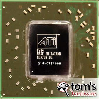
Close-up of the GPU package. From chip size seems to be the successor of the Radeon HD 6600M Series I
source
 
Last edited by a moderator:
Much better. Taking that and assuming a 30mmx30mm package, it more like only 140 mm² (13,64 x 10,27 mm², round up to be on the safe side).

arrive closer to 180mm² for that picture as it includes the kerf area. So the "marketing die size" of the above die may be just about 130mm².

Hmm assuming package size is the same I've rotated and scaled the image and indeed it is somewhat smaller than Juniper so your guess looks about right.

Though without even knowing if that's GCN or not it doesn't say much, other than it should be (given the die size and considering the die shrink) faster than Juniper...
 
Though without even knowing if that's GCN or not it doesn't say much, other than it should be (given the die size and considering the die shrink) faster than Juniper...
Referring to my earlier guess here (I may have switched CapeVerde and Pitcairn), that would fit not too bad to the smallest GCN die with 12 CUs (768 SPs, 48 TMUs) and 16 ROPs on a 128 bit memory controller, which will probably form the HD7700 series (HD7600 will be the same die with 4 CUs deactivated). It would be slightly larger than Turks (118mm², 480 SP, 24 TMUs, VLIW5) but should more than double the performance (and easily passing Juniper, too of course).
 
Launch 6th December?http://www.heise.de/newsticker/meld...-ersten-28-Nanometer-Grafikchips-1361366.html
AMD is apparently planning to introduce the first products using 28-nanometer graphics chips in December 2011. As Heise learned from business circles, it should be in the second week of December so far - a source specifically named the sixth December. Already a few weeks ago, one source said, AMD wanted the chips before 9 December - otherwise, the launch moves into next year.
 
In this day and age, people will believe CGI cartoons first and then (dead) scientists.
 
In this day and age, people will believe CGI cartoons first and then (dead) scientists.

Hmm.. The (dead) scientists reference is probably about Kepler, but the CGI cartoons part I dont get. Anyone wants to help solve the new enigma from Neliz? :D
 
I would guess CGI cartoons refers to the Scorpius AMD FX animations,but not sure about the interpretation ;)
 
So let me get this straight , AMD is moving toward an NVIDIA like architecture (easy to program and mostly hardware scheduler) ?

Or is it moving toward an Intel Larrabee like architecture which had software scheduler and the only difference is that instead of using a 16-wide vector Pentium processors , AMD will design it's own 16-wide vector hardware ?

Or is it a combination of both ? mainly hardware sceduler (NVIDIA's way) and multiple 16-wide vector units (Larrabee's way) ?
Neither nor. Or in between or something else, it depends on what you are looking.

On a very high level it looks a bit like the Cray X1 on a single chip. Four vector processing units (SIMD engine now, SSP in the X1) form a basically self-contained unit (CU or MSP) integrating scalar and vector capabilities. But that's where the similarities end.

GCN inherits the physical width (16 elements) of the vector ALUs almost all GPUs (and Larrabee) use now. The logical width stays at 64, the value used by AMD for quite some time, though. But instead of using one VLIW instruction to issue 4 operations for a single vector (wavefront) as with Cayman, it uses 4 instructions from 4 different wavefronts to fill those vector ALUs. That somewhat resembles a hypothetical doubled GF100 SM with 4 instead of only two vec16 ALUs. The scheduling works different from all formerly known GPUs though.

A GF100 SM has several issue ports (2x vec16 ALU, SFU, L/S [local and global memory]), where each of the two single issue schedulers can issue one instruction for a vector/warp every second (hot) clock cycle (some exceptions apply because of resource contention). Because of the long pipeline (18 cycles or 9 vectors deep) a sophisticated scoreboarding scheme exists to track dependencies between instruction for a warp. For each Warp in flight, a window of 4 or 5 instructions is checked for dependencies and can potentially be issued before another independent instruction for the same warp completes.

R600 through R900 used a far simpler scheduling system. The compiler arranged the instructions in groups (clauses) which were guaranteed to be independent. Control flow or memory instructions opened up separate clauses. Each CU/SIMD engine had two thread sequencer, which simply alternated in supplying the instructions for two wavefronts. Each instruction issued over 4 cycles (64 element warp on vec16 ALUs), this fits exactly the pipeline length of 8 cycles (2 vectors). That means no checking whatsoever had to be done within a clause. For the next instruction 8 cycles later, all dependencies were guaranteed to be resolved. Dependencies were only checked on clause granularity by the global "dispatch processor", making fine grained control flow slow (changing clauses took about 40 cycles, i.e. clauses with less than 10 instructions lower the performance).

GCN does something different. It tries to retain much of the simplicity of the R600 approach with added flexibility and performance. It has basically 4 schedulers within a CU, which work in a round robin fashion (a bit like the alternating thread sequencer in R600). Those schedulers issue to a set of ports with are mostly shared (scalar unit, branch unit, Export/GDS, vector memory, local memory) within the CU but partly private (vector ALU, each scheduler can issue only to its own vec16-ALU) to each scheduler. The shared ports can accept a new instruction each cycle, the private ones only every 4, matching up to the round robin issue.
Up to 5 instructions per cycle can be issued at maximum. Each scheduler selects up to 5 instructions (if there are so many) from 5 different types and from 5 different wavefronts (no dependency checking within a wavefront). Memory dependencies are handled by compiler inserted barrier type instructions counting the number of allowed outstanding memory accesses (which are counted then in the hardware too of course). These barriers disable instruction issue for the wavefront until the dependency is resolved and are consumed within the scheduler itself.
While the GCN approach lacks some of the flexibility of the nvidia scheduler, it makes up for that with the massive amount of issue ports enabling to handle control flow and "scalar stuff" (identical in all elements of the vector) basically in parallel to the vector ALUs increasing the utilization while maintaining a relatively simple operation.

Btw., the main difference between Larrabee (besides the scheduling of Warps/Wavefronts/vectors and that it has a full two issue x86 core as scalar unit per vec16 ALU) and GPUs is that Larrabee has a permute network between register file and the vector ALU lanes. GPUs basically use their local memory for that purpose. In GPUs, each vector lane has its own register file, no such permutations are directly possible. While that decreases flexibility, it saves quite a bit on the power consumption for the reg file.
 
Neither nor. Or in between or something else, it depends on what you are looking...
Thank you very much Gispel , that was an informative read indeed . :smile:

I had to diverge and google search some of the terms you used (round robin , So really what AMD did here is add to their scheduling capabilities to increase their ALU utilization rate , and If I understood your post correctly , the compiler has less to work for now (now that clauses are gone) .

In a hypothetical reality , how much more performance does a GCN core (with 1532 ALUs @880 MHz) achieve over a Cayman core running at the same frequency and with the same number of ALUs ?
 
Last edited by a moderator:
More likely the GPU for the HD7700/HD7600 series.

But considering the performance/power ratio couldn´t it be the base for a console version?. I say so suppossing new consoles will ship in 28 nm and that chip is similar in seize to xenos parent die...
 
Back
Top