I dont know, that's why I asking.
Given the simplistic nature of the diagram and processors' diagrams in general, it shouldnt be hard at all.
Follow along with the video below to see how to install our site as a web app on your home screen.
Note: This feature may not be available in some browsers.
I dont know, that's why I asking.
Are you sure? If so then yeah, MS wouldn't really have a legal case to make to take them down.


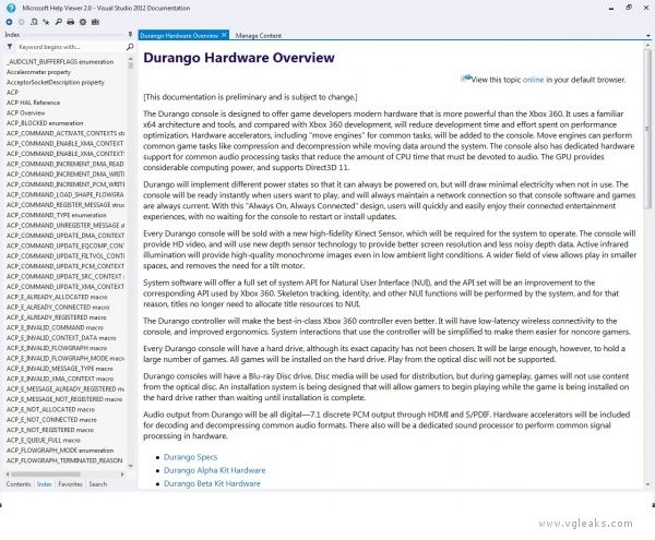
No, even if that was true (redrawing diagrams), they are still copy and pasting screens from the XDK environment:


Nevermind that most of their articles' written content also looks like direct copy and paste from the ATG dos - the guy behind vgleaks is not a native English speaker and it shows in his other posts where he reposts rumours etc.
bkilian suggested they did a while back. The diagrams VGLeaks has been using in their articles come directly from MS documentation iirc. bkilian even mentioned how it was interesting that MS wasn't bothering to take the info down.
No, those diagrams are not made by VGLeaks. Neither is the text written wholly, or even in part, by VGLeaks.The diagrams VGleak is using are self made, ergo not actual copyrighted material.
MS can't take them down, they have no legal claim on a self made diagram.
Im new to this forum and have been reading post he past month. Is it true that Microsoft upgraded from DDR3 to DDR4. I read this a few pages back.
I had a discussion with friends they said it was no way Microsoft can upgrade becaude of the lack of time to do test the chip.
Im new to this forum and have been reading post he past month. Is it true that Microsoft upgraded from DDR3 to DDR4. I read this a few pages back.
I had a discussion with friends they said it was no way Microsoft can upgrade becaude of the lack of time to do test the chip.
Microsoft hasn't shown any willingness to use bleeding edge hardware, so why would they start with RAM?
Where do you get that from?
Considering the previous 2 generations.... Lol
If anything they are the most likely to use bleeding edge hardware
No, even if that was true (redrawing diagrams), they are still copy and pasting screens from the XDK environment:
Nevermind that most of their articles' written content also looks like direct copy and paste from the ATG docs - the guy behind vgleaks is not a native English speaker and it shows in his other posts where he reposts rumours etc.
Point made more of an assumption well spread on the web.Says who, and even if it were offered, why exactly would they have more to offer?
True too but I jump to the next point.Higher R&D for the on-die SRAM pool is a one-time cost, and pretty much everybody knows how to handle SRAM on-die. SRAM can be engineered for high redundancy, so yield impact is not as bad as raw die area would suggest. There's just one chip on the package, and the SRAM will shrink with any node transition.
Well Intel sells it for 50$ because it allows their GPU to breath and may save the laptop manufacturers the cost(s) associated to a discrete GPU. THat is not to say that a 70/80mm^2 of eDRAM would sell for that much. I jump to the next point again.A separate eDRAM die like Intel's is sold for maybe an extra $50 for every unit, and it will not integrate with a die with a standard logic process, meaning it's an extra component even if the main APU shrinks.
Well you got me to wonderAre you certain they'd want to use IBM's process?
