The nvidia future architecture thread (G100/GT300 and such)

That's precisely my point. When setup, fillrate, and BW are equal, game performance isn't affected as much as you'd expect by having double the ALU and TEX. Adding only ALUs will have an even smaller effect.
Trouble is "as much as you'd expect" is ill-defined - clearly G92's extra ALUs and TMUs are bringing a useful performance gain:

http://www.xbitlabs.com/articles/video/display/asus-en9600gt_12.html#sect3

(note: G92 here has a 10% more bandwidth than OC'd 9600GT)

http://www.computerbase.de/artikel/...hd_4850_rv770/20/#abschnitt_performancerating

Though at the same time I personally feel that 50% extra performance is the lowest margin one should pay for when choosing between GPUs.

The point about GT200b is that in comparison with G92b, setup, fillrate and BW will all increase. So when I propose adding ALUs (and TMUs) to G92b (and not forgetting the prodigal MUL and improved efficiency of GT2xx texturing) it's alongside other basic gains in capability.

I'm really intrigued to see what happens with NVidia's ROPs when they get ~double the bandwidth per ROP. They should fly - they've long been strangled by GDDR3.

Again, exactly my point. I don't think adding math to G92b (or, almost equivalently, chopping everything else from GT200) will do much.
NVidia can't lower the ALU:TEX ratio. And don't forget attribute interpolation "silently" consumes some ALU capability - so you can't do a direct comparison with ATI's ALUs/mm.

You do realize that a few sentences before this you attributed G94's speed to its ROPs/BW, right? ;)

If 16 ROPs are useful to a 4 cluster GPU, you can't say 32 ROPs are excessive for a GPU with 10 even faster clusters.
The problem being that G92 is held back by not having enough BW per ROP. Don't forget it nominally has twice RV770's per clock Z rate.

So G94 with 128-bit GDDR5 and 8 ROPs, with twice the bandwidth per ROP, would prolly have been a really nice, and small, thing. Trouble being, of course, the timing of GDDR5.

You can be sure that GT200 would take a hit with half the ROPs, and likewise RV770 would be notably faster with double the ROPs.
I'm not sure what you're saying here - both GPUs would have the same per-clock colour rate, while GT200b would have twice RV770's Z-only rate.

Though, per-Z/per-clock, NVidia's ROPs appear to need an overhaul, even after GDDR5 arrives as MSAA performance seems a bit lacking. Maybe, in adjusting to the burst length of GDDR5 (which is presumably non-trivial), NVidia can get a bump in per-ROP efficiency here?

There's no easy fix here. These adjustments that you're suggesting will change perf/$ by a few percentage points at best. NVidia didn't really make any mistakes in the balance between the execution units. RV770 simply raised the bar on how good each part of a GPU -- TMU, ROP, MC, ALU, TEX, scheduling, etc -- can be for a given silicon budget.
GT200's increased performance per TMU indicates NVidia was using an excess of units in G8x/G9x to attain desired performance.

GT200's increased per-ALU performance with increased register-file size per SIMD indicates that G8x/G9x had too little register file.

NVidia increased the size of batches, which cut the cost of scheduling/operands in GT200 - again it seems NVidia made the batches too small in G8x/G9x - though there are other issues there...

We'll see a similar thing when NVidia introduces GDDR5 - the "excess Z-rate per ROP" will get utilised more effectively.

Jawed
 
Doing both is tough, and the only reason ATI was able to do it was the mediocrity of their previous design.
Performance per-unit in R6xx, though, is clearly very good (excepting excess bandwidth).

Orton, back in 2007 (just before the launch of R600), said they "didn't have the tools" to do what they wanted with R600 - which has always implied to me that units were bigger than they needed to be (and, lower-clocked per watt). I don't think that's all of what went wrong - the ring-bus appears to have been a blind alley.

But if RV770 partly reflects "having access to the tools", then it shouldn't be surprising that there's a magnified effect when comparing the two and looking purely at per-unit die-area.

Jawed
 
Hmm, you appear to be saying that R800 will be a 55nm GPU (presumably in this case two on one board). Presumably the die can't get any smaller than RV770 on 55nm for a 256-bit bus - unless they radically reduce power consumption?

Jawed

According to the rumors R800/RV870 will be on TSMC's 40nm half-node, sorry if I was unclear. NordicHardware, Fudzilla and arstechnica report this. What I meant was that the RV770 would be getting a 40nm refresh as well, but not for the high end. In the high end it's getting a relatively short lifespan.
 
I just want to add that NVidia's focus on "scalar" ALU instructions when building a chip for processing vector data types (with the occasional scalar resource) is very costly. That appears to lie at the heart of a 30-40% increase in die area per FLOP in comparison with RV770 - which presumably is close to "custom" in terms of the efficiency of its implementation.

The issuing of instructions is also very much more fine-grained in NVidia's GPUs than ATI's. NVidia issues individual instructions, whereas ATI issues clauses (though a clause can be as short as a single scalar instruction). NVidia seems to be tracking a hell of a lot more status per batch than ATI - though this is offset somewhat by the fact that ATI has way more batches possibly in flight per SIMD.

Finally, the scalar ALU organisation means that NVidia is forced to have more elements retired per clock - 240 per clock in GT200 versus only 160 in RV770 - even though NVidia is also running the ALUs at ~2x ATI's ALU clocks. This is further exacerbated by NVidia's choice of 8-wide SIMDs, which means that there are 30 SIMDs instead of only 10 in RV770. This adds yet more control overhead.

NVidia's smaller batches (32 elements in comparison with 64) don't appear to be providing a benefit in dynamic branching, e.g. the Steep Parallax Mapping PS3.0 test here:

http://www.ixbt.com/video3/rv770-part2.shtml

is, I believe, heavily dependent on dynamic branching (RV770 is 4x faster per clock than RV670 :oops: ). Though I'd like to see much more analysis of dynamic branching on GT200 and RV770. I suspect RV770 may be benefitting from some texturing-related trickery which inflates DB performance in comparison with RV670.

---

Overall, I think NVidia's going to stick with its ALU architecture.

EDITED: NVidia could "easily" go with 8-clock instructions instead of 4-clock instructions, to arrive at 64-element batches.

Increasing the ALU:TEX ratio also reduces the per FLOP control overhead, since each cluster appears to have some control logic common to all the SIMDs in each cluster.

Apart from that, I think as far as ALUs are concerned, it's a case of getting them to 2GHz and beyond...

Jawed
 
What I meant was that the RV770 would be getting a 40nm refresh as well, but not for the high end. In the high end it's getting a relatively short lifespan.
Hmm, but if RV770 is shrunk, it's going to be pad-limited - or put another way, it can't shrink.

I dunno there might be a small reduction in pads due to reduced power demand, but overall RV770 seems to be I/O pad limited (memory, PCI Express, Displays, CrossFireX Sideport).

Jawed
 
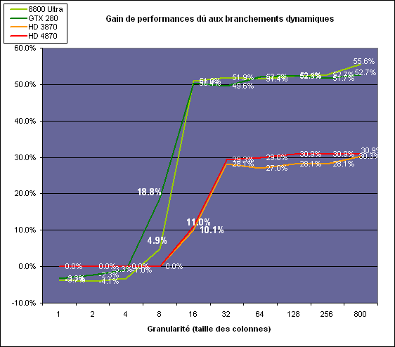
Though I'd like to see much more analysis of dynamic branching on GT200 and RV770.

Here ya go:

img00236261gf3.gif

IMG0023626.gif


Source
 
Last edited by a moderator:
So in pure ALU code there is no difference between RV770 and RV670 - which is a relief.

The question is, is the Steep Parallax Mapping PS3.0 test 4x faster because of dynamic branching (and what I'm guessing is texturing-within-DB-clause improvements) or is there something else going on?

Jawed
 
What about double-precision? AFAIK Nvidia albeit being quite slow on DP supports a wide range including some nifty features with their dedicated HW-units. In my laymans understanding, that should result in a fairly big block of transistors used specifically for this purpose.

Can anyone quantify on those ALUs? Wouldn't it be possible to re-use existing ALU hardware as AMD does? Seems to be the "smarter choice(tm)"… or is something in their structure - maybe even the scalar nature of the NV-ALUs preventing them from being (ab)used for that kind of calculation?


edit:
Another option for Nvidia to gain FLOPS/mm² might be to strip their ROPs and/or TMUs of some (seldom used) functionality that could be emulated via shaders - but I am totally lost as to how many additional shaders would be required until this move would amortize itself
 
Last edited by a moderator:
What about double-precision? AFAIK Nvidia albeit being quite slow on DP supports a wide range including some nifty features with their dedicated HW-units. In my laymans understanding, that should result in a fairly big block of transistors used specifically for this purpose.
Compared to a single-precision unit, the ALUs would be significantly larger. I can't see which section of the shader arrays goes for DP from the die shots I've seen.
The DP unit, at least as I've seen it described, blocks SP register access, so that cost is shared.
Other parts of the shader arrays contribute significantly to die area, such as the register file, special function unit, and scheduling hardware.
DP adds space, but it is it enough to explain the full density disparity between RV770 and GT200?
Discussions elsewhere peg the blame more on the more involved scheduling and instruction issue per ALU than the DP sections.

Can anyone quantify on those ALUs? Wouldn't it be possible to re-use existing ALU hardware as AMD does? Seems to be the "smarter choice(tm)"… or is something in their structure - maybe even the scalar nature of the NV-ALUs preventing them from being (ab)used for that kind of calculation?
DP for AMD was a cheaper leap to make, as there were already operations that linked together pairs of SP ALUs. DP would be an elaboration on that.
Perhaps that was the plan all along, or a happy side effect of the superscalar arrangement.
Whether it's entirely optimal, I don't know.

Nvidia's DP unit has significantly more functionality tacked on, such as denormal signaling and fully-fleshed out rounding--the sorts of things that add nothing to peak performance and bloat the transistor budget, but go a long way in making GPU DP more broadly applicable.

It's one thing to add all the extra hardware to a dedicated unit. The cost can be contained.

Doing the same for AMD would involved instrumenting and rewiring entire shader arrays.

edit:
Another option for Nvidia to gain FLOPS/mm² might be to strip their ROPs and/or TMUs of some (seldom used) functionality that could be emulated via shaders - but I am totally lost as to how many additional shaders would be required until this move would amortize itself
I'm pretty sure the balance of hardwired logic and emulation is evaluated all the time.
A bad guess can lead to either strangled FPS/mm² or bad FLOPS/Watt.
Power is already a first-order constraint on designs, and it's going to be an even bigger talking point come 2010, if some of the shaky rumors on future hardware turn out to be true.
 
since the G92(b) came up quite often as a performance baseline: I seem to recall it has a 0.5tri/clock setup rate, opposed to the 1tri/clock rate for GT200 and the ATI cards. this may explain the relatively low difference between G94 and G92 (although I'm quite sure BW is a factor too).
 
So in pure ALU code there is no difference between RV770 and RV670 - which is a relief.

The question is, is the Steep Parallax Mapping PS3.0 test 4x faster because of dynamic branching (and what I'm guessing is texturing-within-DB-clause improvements) or is there something else going on?
Actually, there is a DB improvement. If you look back, there are some DB tests where RV670 did worse than R600. Maybe there was a bug or shortcut to save space or something.

However, RV770 is back to R600 levels on a per-ALU basis.

http://www.digit-life.com/articles3/video/rv670-part2-page1.html
http://www.ixbt.com/video3/rv770-2-part2.shtml

When compared to R600, it's a 2.5x increase. Similar results here:
http://www.xbitlabs.com/articles/video/display/radeon-hd3870-hd3850_16.html#sect0
http://www.xbitlabs.com/articles/video/display/ati-radeon-hd4850_17.html#sect0
 
Actually, there is a DB improvement. If you look back, there are some DB tests where RV670 did worse than R600. Maybe there was a bug or shortcut to save space or something.
However, RV770 is back to R600 levels on a per-ALU basis.

http://www.digit-life.com/articles3/video/rv670-part2-page1.html
http://www.ixbt.com/video3/rv770-2-part2.shtml
Hmm, is it possible to eliminate bandwidth though? Bandwidth is the only factor of an equivalent magnitude between R600 and RV670.

I presume you're referring to the same Steep Parallax Mapping PS3.0 test that I referred to, earlier. As I mentioned earlier I think there's some trickery related to the evaluation of textures when there's incoherence in a batch (of 64 fragments). I suspect this patent document is the key:

Method and apparatus for moving area operator definition instruction statements within control flow structures

and thus would explain the huge boost in performance. One thing I'm not clear on is whether this technique is hardware dependent (as most of the talk is about compilation). I haven't read the document closely enough.

Sadly the Hardware.fr tests for DB seem to have changed since the R600 results were published:

http://www.hardware.fr/articles/671-5/ati-radeon-hd-2900-xt.html

Hardware.fr appears to be the only place with any kind of pure-ALU test of DB.

Again texturing and/or bandwidth could be big factors here... The "Heavy Dynamic Branching" test shows less advantage for HD2900XT over HD3870 than the other tests which are listed as having texturing techniques (40% versus 64% and 69%).

Jawed
 
Hmm, is it possible to eliminate bandwidth though? Bandwidth is the only factor of an equivalent magnitude between R600 and RV670.
I don't see how BW can be a factor when the 4850 has even less than the 3870 yet outperforms it by a factor of 4. RV670 seems to have a DB bug, as shaders using this are the only ones where R600 is much better than RV670.

Again texturing and/or bandwidth could be big factors here... The "Heavy Dynamic Branching" test shows less advantage for HD2900XT over HD3870 than the other tests which are listed as having texturing techniques (40% versus 64% and 69%).
Maybe the bug/deficiency only kicks in when texturing instructions lie in the branch, but BW can't be an issue.

Nonetheless, my main point is that branching isn't really any better in RV770 than R600. The only tests that show a slight per-clock per-ALU edge are those xbitlabs shaders.
 
I don't see how BW can be a factor when the 4850 has even less than the 3870 yet outperforms it by a factor of 4.
I'm interpreting the patent to be exclusive to RV7xx. With a reduction in texture fetches (hence bandwidth) there's an increase in throughput.

Dunno, the code would help. This is the best I can find:

http://graphics.cs.brown.edu/games/SteepParallax/index.html#shaders

which contains two dynamic loops each of which contains a dependent texture fetch. ( :cry: I can't make this shader compile in GPUSA :cry: ).

Now, having looked at this code it seems that the patent I linked earlier may not be relevant - I'm out of my depth as I don't understand the patent in detail and whether it would be applicable to this code. I think not, because texturing is not gradient based.

RV670 seems to have a DB bug, as shaders using this are the only ones where R600 is much better than RV670.
Well ixbt hypothesises bandwidth as a possibility, too.

Maybe the bug/deficiency only kicks in when texturing instructions lie in the branch, but BW can't be an issue.
Well, maybe it's a ring-bus bandwidth issue then, since ring bus scales with the size of the memory bus. Remember that TUs in R6xx are shared by all SIMDs, and it seems that texture results are distributed to SIMDs by the ring bus. So if RV670 has "half" the ring-bus bandwidth of R600, then this might be the bandwidth bottleneck, which is a function of the kind of dependent texturing in this test.

I'm not sure how incoherent the texturing in this shader is though.

Nonetheless, my main point is that branching isn't really any better in RV770 than R600. The only tests that show a slight per-clock per-ALU edge are those xbitlabs shaders.


The three tests:
  • DB = 269% = 8% faster per clock
  • DB + 10 textures = 278% = 11% faster per clock
  • Heavy DB = 296% = 18% faster per clock
Jawed
 
since the G92(b) came up quite often as a performance baseline: I seem to recall it has a 0.5tri/clock setup rate, opposed to the 1tri/clock rate for GT200 and the ATI cards. this may explain the relatively low difference between G94 and G92 (although I'm quite sure BW is a factor too).

I've not heard this. I believe all modern GPUs are a full poly/clk setup.
 
Well ixbt hypothesises bandwidth as a possibility, too.
Only because as far as we know that's the only difference in architectures.

Well, maybe it's a ring-bus bandwidth issue then, since ring bus scales with the size of the memory bus. Remember that TUs in R6xx are shared by all SIMDs, and it seems that texture results are distributed to SIMDs by the ring bus. So if RV670 has "half" the ring-bus bandwidth of R600, then this might be the bandwidth bottleneck, which is a function of the kind of dependent texturing in this test.
Then we would have seen R600 outdo RV670 in other texturing-heavy tests. This deficit only applies when branching is involved.

The three tests:
  • DB = 269% = 8% faster per clock
  • DB + 10 textures = 278% = 11% faster per clock
  • Heavy DB = 296% = 18% faster per clock
Jawed
Yup, and even some of that is due to driver/compiler improvements (RV670 scores are improved a few percent in the 4850 review). Or did you already account for that?

You can also see similar patterns in the digit-life shaders.
 
Back
Top