Install the app
How to install the app on iOS
Follow along with the video below to see how to install our site as a web app on your home screen.
Note: This feature may not be available in some browsers.
You are using an out of date browser. It may not display this or other websites correctly.
You should upgrade or use an alternative browser.
You should upgrade or use an alternative browser.
Ray Tracing Versus Rasterization, And Why Billions Of Dollars Is At Stake
- Thread starter Brimstone
- Start date
Jawed
Legend
So, finally, once you've got unified ultra-high-performance, ultra-flexible memory and the ability to design programmable cores with any combination of latency/bandwidth trades and vector/scalar computations, which bits of the "fixed function" ray-tracing hardware implementation are left over?
Jawed
Jawed
Who's going to design the programmable cores, and evaluate the tradeoffs? No resource is infinite; design and optimization skills will still be in demand. Tho in the future you posit, ATI seems very well situated to participate. They've got a guaranteed seat at that table. Where is NV in that future?
Jawed
Legend
My point of view with respect to ATI is that they're demonstrably closer (than NVidia) to building the "data parallel processor with graphics gubbins tacked on".
Then it's a question of what kind of computing you put inside that architecture? FP, integer, scalar, vector, and the degree of threading granularity. Clearly you don't just knock one of these off every 6 months - but I think it's fair to say that ATI's spent a few years now covering a fair chunk of ground.
In effect, GPUs have become a tight constraint on the expertise that ATI's developed. Admittedly GPUs are going to continue to get more general-purpose (e.g. supporting virtual memory) but it must also be very tempting to sell DPPs for other purposes and make tighter bonds at the system level.
Ultimately what I'm suggesting is that the kind of expertise ATI is developing could be put to good use building a programmable ray tracing processor. It may not be called that, it might merely be a specific configuration of a DPP. Maybe there'd be a call for fixed function hardware in there (in a similar way to TMUs) designed for ray tracing (hugely dependent on the kind of data structures employed?).
By the time this is possible, ATI's DPPs will presumably be so closely associated with AMD's CPUs that they'll barely be distinguishable.
I don't see any reason why NVidia hasn't been doing this kind of work - NVidia seemed to make the first noises about GPGPU a few years back (on the back of NV30's FP32 and long-shader support), so it may be just a question of timing/resources/priorities.
Jawed
In five years' time we could be looking at systems that use wireless buses. Suddenly the point-to-point restrictiveness of ultra-high-speed memory buses disappears.
With all due respect... My very personal opinion on this is that you may have been too eagerly smoking something.
")
Do you seriously mean 'wireless' as in 'through the air'?
There's going to be 2 major problems for data intensive chips: power and memory bandwidth.
The number of transistors is still increasing faster than the rate at which data can be fed into the chip and the power consumption/mm2 is increasing also. Your biggest problem is that you may end up with too many transistor with too little to do due to the limitations above.
- There's no way your going to get similar bandwidths, since your theoretical maximum bandwidth is a direct function of S/N, which is far higher for wires than for wireless transmissions. The closer you want to go to your theoretical BW, the harder it becomes. Almost exponentially.
- To obtain the maximal bandwidth, you'll need to transmit at high power (to increase your S). More power. Bad.
- You'll need to use advanced error coding (RS, Turbo). Lots of toggling FF's. Lots of area. Bad.
- Advanced coding inherently means increased latency. *A lot*. Which results in deeper buffers. Even more area. More bad.
In fact, within 5 years, no amount of technological advances are going to get you even close to current bandwidths. Even simple 802.11b transceivers need a serious amount of DSP power to get their job done.
You weren't serious, were you?
Now if you'd said optical. Maybe. 10 years from now or so.
Another thing to consider is that x86 cores have fairly lowsy floating point performance because they're focussed on correctness, IEEE, double-precision, the works.
(I assume we're not talking about the stack based x86 FPU, which is broken due to obvious reasons.)
The x86 FP performance is worse than some other processors (especially Itanium and Power5), but this has nothing to do with correctness, DP and IEEE compliance: those other processors have to do be compliant as well. Which makes me assume that you're comparing against non-traditional processors...
Then, of course, CELL comes to mind. But the trend is against you here. I can't think of a single FPU unit that hasn't evolved, over time, from non-compilant single precision FP to compliant double precision FP. There's good reasons for that:
- Double precision is a very important checkmark in the scientific and engineering community. Correct rounding even more so: they simply laugh you away if you don't have it. I don't expect CELL as it is to be deployed at lot in the S & E community for exactly this reason.
- The incremental cost of double precision and rounding is relatively small. And shrinking. Clearly the multipliers and adders are a solved problem. Additional cost close to zero. The rounding is fairly complicated but not excessive.
- Register files need to double in size, but that's also a fairly small area hit.
- These days, with interconnect now the major delay factor, it's typically not in the main critical path of the overall pipeline anymore.
The other logic stays largely the same. There's no real need to beef up the memory system: sure, your number of FLOPS will be lower in DP mode than in SP when going to external memory, but that's the programmer's choice, just the way it currently is for a CPU.
The other GPU-specific engine that aren't used during GPGPU mode can safely remain SP.
So assuming you're still talking about GPU's, I don't believe for a second that the overall area impact will be double.
Surely it can't be long before Intel decides it's time to put in some single-precision pipelines and steal-back some of the glory that Cell's taken?
Don't count on it. It's not going to happen. For a pure processor, it'd be commerical suicide.
At the same time, ATI knows it is practically impossible to compete on Intel's home turf: double-precision. That complexity may never come to GPUs, it's utter over-kill and immensely costly in terms of transistors (well over 2x I think).
If double precision never comes to the GPU, it will be because the grand vision of the GPU as a massive parallel general purpose calculation engine didn't materialize.
If however that vision does become true and becomes a feature that can make good money, expect full compliant double precision to arrive quickly. DP is a solved problem. It's not complicated (and, with a standard that's been frozen for years, not getting more complicated), it's not overkill and it's not very costly.
In five years' time we could be looking at systems that use wireless buses. Suddenly the point-to-point restrictiveness of ultra-high-speed memory buses disappears.
No pun, but I sincerely expect to see pigs fly before I see wireless busses in such a role.
Jawed
Legend
Clearly I aint qualified on this stuff
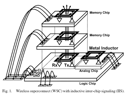
Analysis and Design of Inductive Coupling and Transceiver Circuit for Inductive Inter-Chip Wireless Superconnect
I was actually envisaging a broader scale wireless infrastructure - one not dependent on chip stacking (where discrete channels are almost in contact), but something more like a conventional 2D layout on a circuit board. The paper describes something that is effectively point-to-point and clearly I'm thinking of something that's not.
As to DP versus SP - for consumer applications, what is the point of DP? I don't know what the relative costs would turn out to be, but in a DPP if you have a choice between a 256-pipe SP or a 96-pipe DP why build the latter (for the same number of operations per second)? A consumer application doesn't obviate an alternative scientific DPP. The two could sit side by side in the catalogue.
But do ray-tracing, game physics, game graphics or AI need DP? As far as I can tell a lot of the emphasis here is on the data-parallel part (ultra high bandwidth, SIMD/vector) rather than precision, per se.
If IBM can contemplate separate SP and DP Cell processors, why can't AMD and Intel?
Is Clearspeed on a collision course with AMD/IBM/Intel?
Jawed
Analysis and Design of Inductive Coupling and Transceiver Circuit for Inductive Inter-Chip Wireless Superconnect
A wireless bus for stacked chips was developed by utilizing inductive coupling among them. This paper discusses inductor layout optimization and transceiver circuit design. [...]
A test chip was fabricated in 0.35-[micrometre] CMOS technology. Accuracy of the models is verified. Bit-error rate is investigated for various inductor layouts and communication distance. The maximum data rate is 1.25 Gb/s/channel. Power dissipation is 43 mW in the transmitter and 2.6 mW in the receiver at 3.3 V. If chip thickness is reduced to 30-[micrometre] in 90-nm device generation, power dissipation will be 1 mW/channel or bandwidth will be 1 Tb/s/mm2.
I was actually envisaging a broader scale wireless infrastructure - one not dependent on chip stacking (where discrete channels are almost in contact), but something more like a conventional 2D layout on a circuit board. The paper describes something that is effectively point-to-point and clearly I'm thinking of something that's not.
As to DP versus SP - for consumer applications, what is the point of DP? I don't know what the relative costs would turn out to be, but in a DPP if you have a choice between a 256-pipe SP or a 96-pipe DP why build the latter (for the same number of operations per second)? A consumer application doesn't obviate an alternative scientific DPP. The two could sit side by side in the catalogue.
But do ray-tracing, game physics, game graphics or AI need DP? As far as I can tell a lot of the emphasis here is on the data-parallel part (ultra high bandwidth, SIMD/vector) rather than precision, per se.
If IBM can contemplate separate SP and DP Cell processors, why can't AMD and Intel?
Is Clearspeed on a collision course with AMD/IBM/Intel?
Jawed
Last edited by a moderator:
In five years' time we could be looking at systems that use wireless buses. Suddenly the point-to-point restrictiveness of ultra-high-speed memory buses disappears.
Jawed
Legend
That supercomputer prolly derives most of its DP capability from Clearspeed chips.
http://www.beyond3d.com/forum/showthread.php?t=33410
Jawed
http://www.beyond3d.com/forum/showthread.php?t=33410
Jawed
Who needs ray-tracing when you can have radiosity!
http://www.geomerics.com/index.php?page=lighting
Who remembers this?
http://www.geomerics.com/index.php?page=lighting
Who remembers this?
http://www.research.ibm.com/actc/workshop2006/perrone.pptThat supercomputer prolly derives most of its DP capability from Clearspeed chips.
http://www.beyond3d.com/forum/showthread.php?t=33410
Jawed
page.7
and:
http://www-128.ibm.com/developerwor...reeDisplayType=threadmode1&forum=739#13859749
Jawed
Legend
But Cell DP doesn't exist yet... Otherwise we'd have heard about it.
If you run the DP numbers:
Clearspeed - 32,000 (2 per board) @ 25 GFLOPs : 800 TFLOPs
Cell - 16,000 @ 31 GFLOPs : 500 TFLOPs
Opteron - 16,000 @ 12 GFLOPs: 200 TFLOPs
Total of 1.5 TFLOPs - being a bit generous there...
Jawed
(feeling embarrassed counting GFLOPs)
If you run the DP numbers:
Clearspeed - 32,000 (2 per board) @ 25 GFLOPs : 800 TFLOPs
Cell - 16,000 @ 31 GFLOPs : 500 TFLOPs
Opteron - 16,000 @ 12 GFLOPs: 200 TFLOPs
Total of 1.5 TFLOPs - being a bit generous there...
Jawed
(feeling embarrassed counting GFLOPs)
"On this day in 2006, someone managed to nonplus Simon F on a forward-looking technical point. World-wide disaster was only averted by quick action of international institutions."
But Cell DP doesn't exist yet... Otherwise we'd have heard about it.
If you run the DP numbers:
Clearspeed - 32,000 (2 per board) @ 25 GFLOPs : 800 TFLOPs
Cell - 16,000 @ 31 GFLOPs : 500 TFLOPs
Opteron - 16,000 @ 12 GFLOPs: 200 TFLOPs
Total of 1.5 TFLOPs - being a bit generous there...
Jawed
(feeling embarrassed counting GFLOPs)
there are 4 different architectures in your guess: x86-64, PPC, SPU, Clearspeed, why not just x86-64 + Clearspeed and Cleap? and it is hard to believe ClearSpeed have not a press release on this project if IBM choice them .
if it is CELL DP not the DD3 CELL(2005) , that will be clear :
CELL DP @ 2.8GHz : 1.4336 PFLOPS
Rev.G K8 Dual Core : 0.1792 PFLOPS
Total: 1.6128 PFLOPS
Jawed
Legend
Clearspeed is already signed up to this architecture of IBM's:
http://www.clearspeed.com/pressreleases/Clearspeed -- ibm 62706 final.pdf
The cynical side in me sees the press release from IBM as promoting Cell specifically. There's no explanation for how 16,000 Cells reach the stated performance.
But it could easily be that the first iteration uses standard Cells and "pin-compatible" Cell DPs are substituted when they're ready in 2008.
Jawed
What would be the point in putting more than 4 x86 cores on a single chip? And the speed improvements are stagnant, while the die area is still growing fast. You need to be able to put something on it that makes good use of it and brings in more money.
With the increase in die area, within 2 generations it might be feasible to put a high-mid end GPU on the die and have plenty of space left over for local storage memory, thereby reducing the bandwidth demand and area needed for cache memory.
And I agree with Jawed, that a unified GPGPU, that can do general DP as well would be best. And it would allow Intel and AMD to strip the FP and MMX/SSE units from the CPU cores, freeing up again about half the area they would otherwise have taken.
Those units are mostly a waste of transistors anyway in that case. They already are when you plump down 4 x86 cores, as you cannot fill all those pipes in any case as it is.
Cell wasn't so stupid after all, it seems.
Clearly I aint qualified on this stuff
Analysis and Design of Inductive Coupling and Transceiver Circuit for Inductive Inter-Chip Wireless Superconnect
I was actually envisaging a broader scale wireless infrastructure - one not dependent on chip stacking (where discrete channels are almost in contact), but something more like a conventional 2D layout on a circuit board. The paper describes something that is effectively point-to-point and clearly I'm thinking of something that's not.
Nice find!
But this paper contains pretty much all ammunition to shoot down the wireless idea. Following the honored tradition of academic paper double speak, it says 1mw/channel or 1Tb/mm2. Not really too bad, but that's assuming a distance of 30um between transmitter and receiver. Clearly you're going to get issues doing this with a GPU linking to multiple memory chips.
Unfortunately, the distance is the key problem. Look as figure 16 to see how the bottom falls out of the SNR number when distance is increased to a mere 400um. Impossible to recover that unless you plan to use the coding techniques that I mentioned earlier and drastically increase the transmit power. Think about what'd be needed to cover mm's instead of um's.
And check out the BER numbers: I don't know the numbers for current memory interfaces, but surely the error rate is multiple orders of magnitudes better than 10er-10. At 1.25Gb/s that's still one error every second.
This paper proposes a really neat idea and who knows it may have some practical applications, but for now I'd classify in under the category 'Fun projects to keep Ph.D. students and their professors busy'.
But do ray-tracing, game physics, game graphics or AI need DP? As far as I can tell a lot of the emphasis here is on the data-parallel part (ultra high bandwidth, SIMD/vector) rather than precision, per se.
Probably not. But the question is only if the incremental cost can be recouped by opening up additional very high-margin markets. Since CELL is mainly used for PS3, intended to sell 10's of millions, the additional cost of DP may not be worth it. But for high-end GPU's, the equation is probably very different. (Does anyone know the lifetime volumes of, say, an R580 or G71?)
If IBM can contemplate separate SP and DP Cell processors, why can't AMD and Intel?
Assuming there exists a DP Cell, note that IBM went from SP to DP. Not the other way around.
Similar threads
- Locked
- Replies
- 10
- Views
- 2K
- Replies
- 37
- Views
- 3K
- Replies
- 608
- Views
- 97K
- Replies
- 90
- Views
- 18K