Jaws said:
This is not wild speculation!

...These are high level possibilities and all are feasible designs. This is why I don't undertsand how E is possible and why I asked the question.
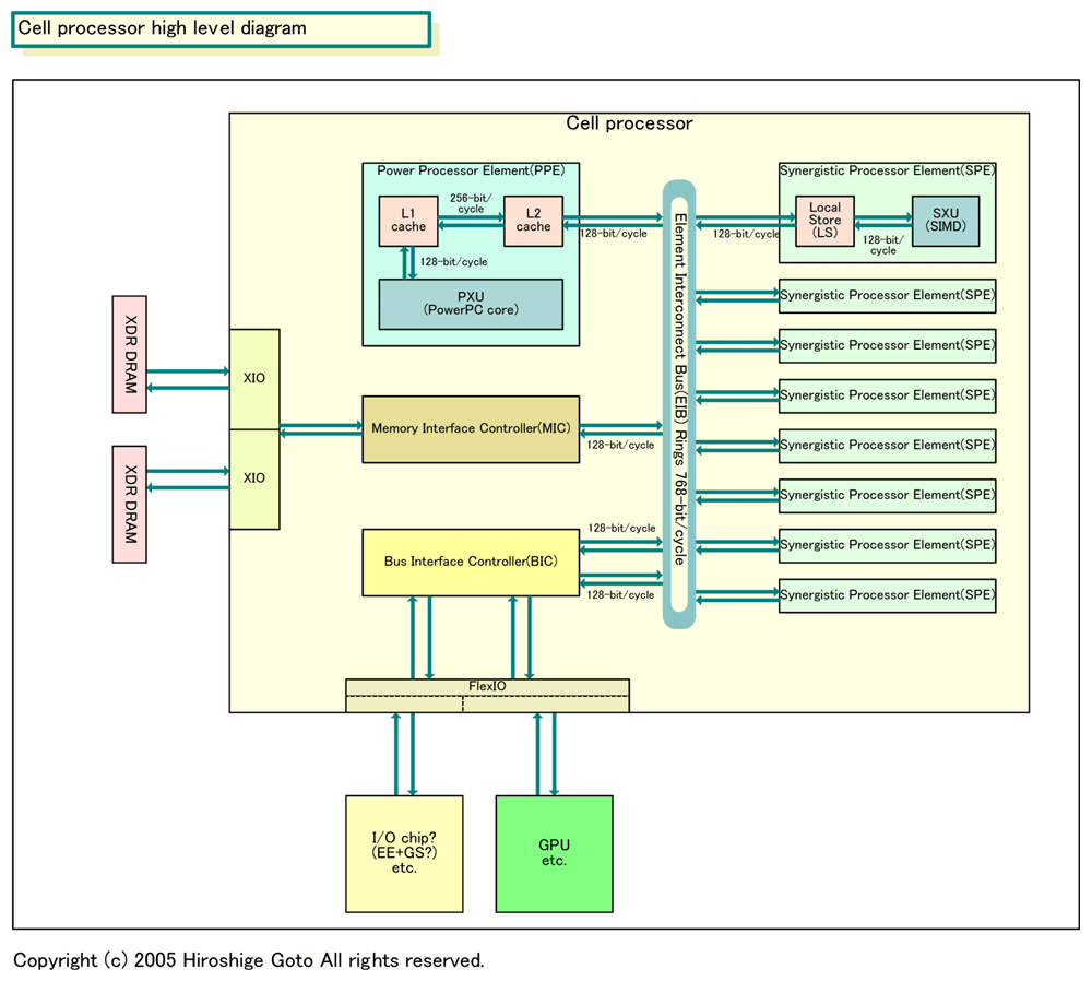
The XIO is the memory interface designed by Rambus so if the CPU or GPU are going to have RDRAM, then it will be off an XIO or similar interface.
I could see an E type in the form of a CELL die, where CELL = CPU + GPU. The XIO would be on the CELL and the shared memory hanging off it would describe E, no?
Otherwise E is either a C or a D depending on how you define it, no?
Well i'm not too knowledgeable on this XIO business, but having one bus to the RAM from CPU and one bus to the same pool from the GPU is feasible, unless i'm missing something.
D has one pool, one bus to the CPU and a separate pool with its own bus to the GPU.
C has one pool, one bus to the CPU and texture data needs to go through the CPU.
E has one pool, 2 busses, one for CPU and one for GPU.
If it's feasible, this should be the best option.