This is a math and font rendering test. This is not a game engine test.
Font rendering eh. Performance difference in Remedy's Control explained.
This is a math and font rendering test. This is not a game engine test.
Other notable references: Legend of the Dragoon, Omega Boost (I d LOVE a proper next gen sequel), Arc the Lad, Xtreme, Twisted Metal, Jumping Flash, Motor Toon, Colony Wars, G-Police, Vib Ribbon, Medievil, Syphon Filter, The Getaway, Primal, Siren, Ghosthunter, Mark of Kri.....there are so many games that came from Sony's owned studios, that were abandoned
Yes Klonoa was amazing. The gameplay is very refreshing and super fun. I wish we saw more of that franchise. But it was produced by Namco I think.
I want to check that out. Does anyone remember the name?


New Dream is over...
Well, I guess they might have just cut some instruction sets, Sony thinks that are not needed for games. E.g AVX is really energy hungry. Might be something sony get rid of, so the CPU does not draw all the power away from the GPU. This is just an example, why they might have cut some things.Dream is over...
What exactly he mean with "parts missing" in the FPU?
Different may also mean that it was altered for the better, right? Because makes no sense to get a Zen 2 CPU and make it worse.
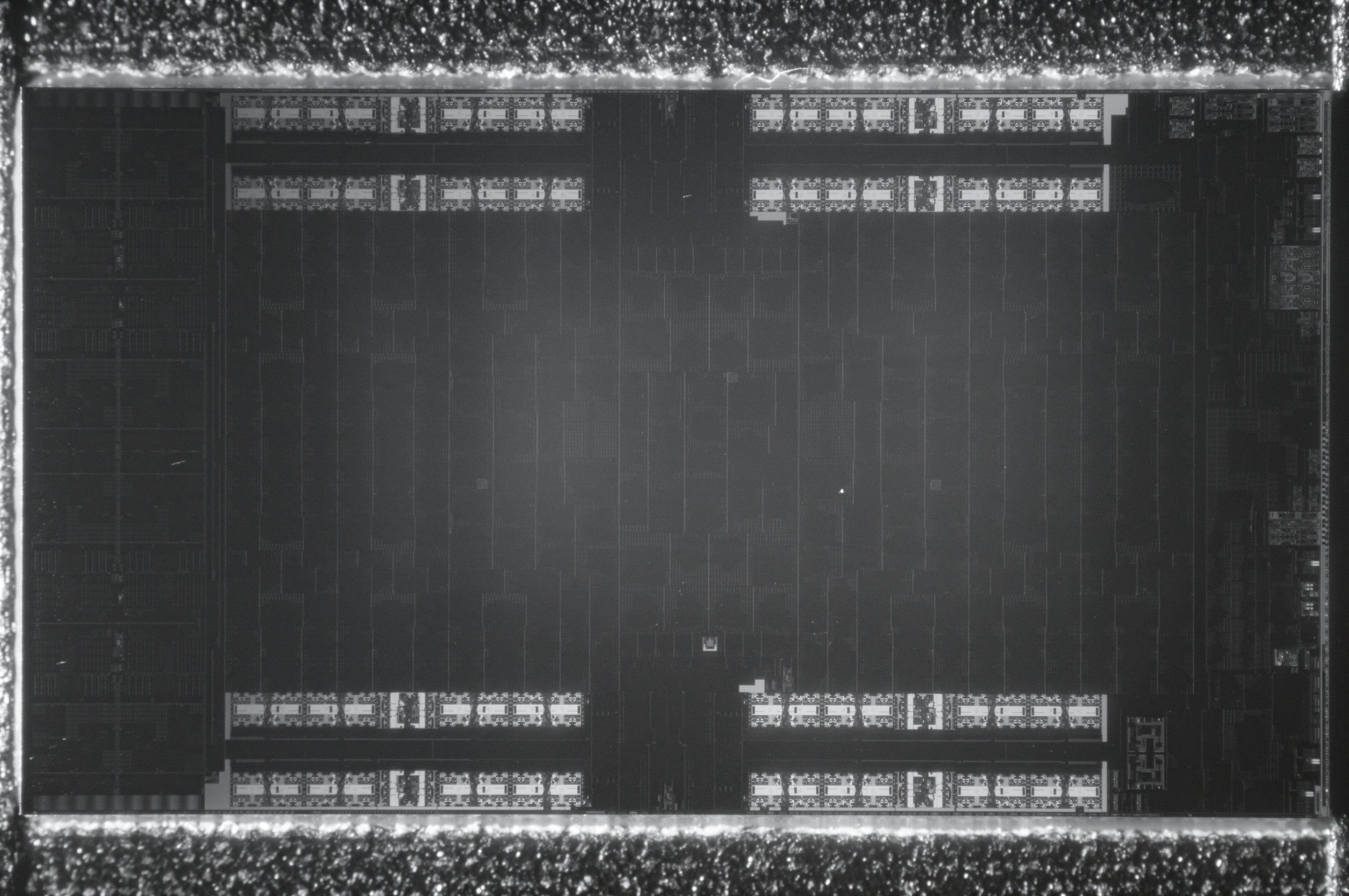
So, the first die shots of the PS5 APU are available
Fritzchens Fritz auf Twitter: "A first quick and dirty die-shot of the PS5 APU (better SWIR image will follow). It looks like some Zen 2 FPU parts are missing. https://t.co/PefXCxc3G1" / Twitter
Maybe someone can point out, what is which part of the GPU, CPU, ...

Edit:
seems like caches are still split, so no infinity-cache (never really expected that).
Surprised to see it is designed exactly as most expected really and there is IC/Zen3 cache missing. RGT and that Moore guy has some explaining to do.So, the first die shots of the PS5 APU are available
Fritzchens Fritz auf Twitter: "A first quick and dirty die-shot of the PS5 APU (better SWIR image will follow). It looks like some Zen 2 FPU parts are missing. https://t.co/PefXCxc3G1" / Twitter
Maybe someone can point out, what is which part of the GPU, CPU, ...

Edit:
seems like caches are still split, so no infinity-cache (never really expected that).

Well, I guess they might have just cut some instruction sets, Sony thinks that are not needed for games. E.g AVX is really energy hungry. Might be something sony get rid of, so the CPU does not draw all the power away from the GPU. This is just an example, why they might have cut some things.
the only thing that comes to mind is AVX. Not sure what else is included in the Floating Point Unit for Zen.Dream is over...
What exactly he mean with "parts missing" in the FPU?
Different may also mean that it was altered for the better, right? Because makes no sense to get a Zen 2 CPU and make it worse.
Well, I guess they might have just cut some instruction sets, Sony thinks that are not needed for games. E.g AVX is really energy hungry. Might be something sony get rid of, so the CPU does not draw all the power away from the GPU. This is just an example, why they might have cut some things.
Maybe they've cut the AVX unit back to 128-bit? Should save some die and ensure significantly lower peak power draw...?
Surprised to see it is designed exactly as most expected really and there is IC/Zen3 cache missing. RGT and that Moore guy has some explaining to do.
This Zen 1 diagram.Maybe they've cut the AVX unit back to 128-bit? Should save some die and ensure significantly lower peak power draw...?

I wonder how people are able to recognize architecture from those pictures
I get what you're saying but isn't this idea totally little insane? Makes no sense, AVX is useful and I don't believe the work to remove instructions from the transistors in the FPU isn't worthy.
Also, Zen 2's energy consumption on 7nm shouldn't be a problem on a high performing hardware.
The vector width of AVX must conform to the standard, unlike SVE or RV64V. Also there’s SSE that takes care of 128-bit.Maybe they've cut the AVX unit back to 128-bit? Should save some die and ensure significantly lower peak power draw...?
This Zen 1 diagram.

I'll be honest in saying, using only your eyes, I think you'd likely only be able to notice the FPU was missing entirely, the likelihood someone could differentiate between 128 and 256 on this is pretty nuts from an x-ray; that's one hell of a call I should say. I'd be hesitant to even make it without verifying with others.

locuza_ said:My interpretation of the floor plan PS5 floor plan:
1. Bomba surprise that Sony likely cut down the 256-Bit FP pipes to just 128-Bit.
2. No Infinity Cache/L3$, also not on the Xbox Series.
3. Might have the old Render Backend design, need higher res to say for sure.
4. The WGPs are arranged as on RDNA1 GPUs with two sub-arrays.
Same goes for the Xbox Series.
Navi21/22/23, Van Gogh and Rembrandt only have one sub-array for all WGPs.
5. Higher res needed for a closer FPU look, GPU frontend analysis and details like the Tempest Audio engine.
hmm.. interesting. Well I can't see shit. So I'll wait for the internet sleuths to put something together.When Zen 2 came out the 256FPU was very obvious and easy to see on the dieshots. It looked like the Zen 1 FPU was mirrored.
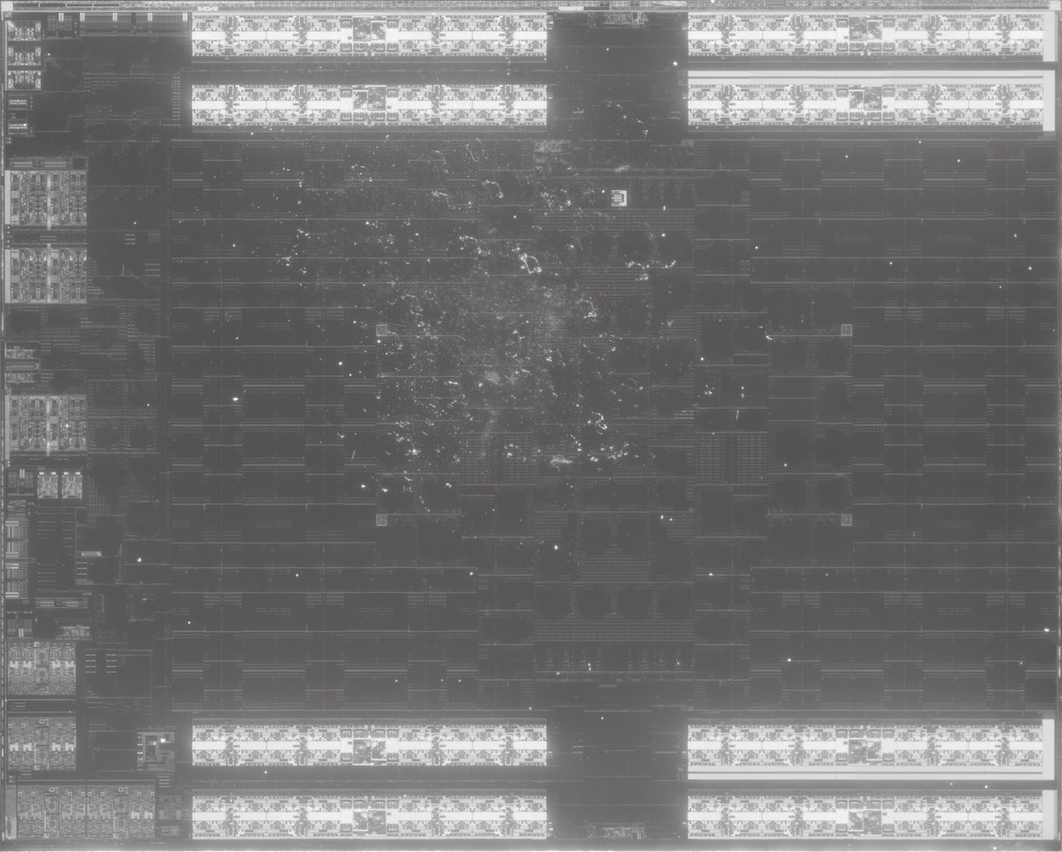
Found this Renoir dieshot with annotations. Fritz image is hard to see, but we can see enough to noticed that the FPU looks "thinner"?

