Install the app
How to install the app on iOS
Follow along with the video below to see how to install our site as a web app on your home screen.
Note: This feature may not be available in some browsers.
You are using an out of date browser. It may not display this or other websites correctly.
You should upgrade or use an alternative browser.
You should upgrade or use an alternative browser.
PlayStation 4 (codename Orbis) technical hardware investigation (news and rumours)
- Thread starter Love_In_Rio
- Start date
- Status
- Not open for further replies.
So how exactly is it that the PS4 can, as a whole, be significantly smaller than the competitor (with an internal power brick vs external) and still command a technical advantage?
In terms of the board the most obvious difference is RAM.
- the PS4 has ~1cm between the RAM and the APU.
- the XB1 has a gap of ~3-5cm? between RAM and the APU.
That's a massive waste of space (needed to match the trace lengths and/or help mount the massive heatsink?).
In terms of 'height', it's simpler - the XB1 has the fan mounted on top of the heatsink, the PS4 has the fan mounted alongside it.
If they were in 32bit mode, probably, but they are in clamshell, each chip has only half the interface to drive. Most of the power goes into the interface.Each GDDR5 chip should consume 1.75 watts if it is produced at 46nm litography so times 16 and you get 28 watts.
If they were in 32bit mode, probably, but they are in clamshell, each chip has only half the interface to drive. Most of the power goes into the interface.
A question, is GDDR chips included into TDP of PlayStation 4 or not?
A question, is GDDR chips included into TDP of PlayStation 4 or not?
TDP is usually specified for the power draw of a particular chip so while each GDDR5 chip has it's own TDP there is no overall TDP for the system. We don't have the TDP for the PS4 APU and will probably never get it from official channels (chip works or some other site may reverse engineer that info though). We also don't have the total system power draw for the PS4 yet (or XB1 for that matter).
Funny that before Sony showed the insides of the PS4 people seemed to think that they knew the full story of the PS4 specs, now that it's been shown we have even more questions.
like
What is that 3rd chip for.
Why is the SoC around 350mm^2 when the GPU & CPU shouldn't add up to being that size.
How much memory does the secondary chip have.
& so on.
like
What is that 3rd chip for.
Why is the SoC around 350mm^2 when the GPU & CPU shouldn't add up to being that size.
How much memory does the secondary chip have.
& so on.
Because Xbox One SoC has eSRAM & the Shape/other Audio Chip on the Die while the PS4 will use GDDR5 off the chip so it doesn't need eSRAM to make up for slow main RAM & I'm guessing the PS4 Audio Chip isn't as big as the Shape & other Audio Chip in the Xbox One SoC.
PS4 has 6 more CUs and Xbox One has 32MB eSRAM.
I remember doing the relative math and the 32MB eSRAM ended up being larger than 6CUs.
Thus PS4 having a smaller APU isn't surprising.
There are some additional questions, but at this point they are trending towards wondering about minor things.Funny that before Sony showed the insides of the PS4 people seemed to think that they knew the full story of the PS4 specs, now that it's been shown we have even more questions.
The chip mounted on four sides with wires could be a microcontroller for miscellaneous peripherals.What is that 3rd chip for.
That kind of mounting doesn't promise a high-performance connection to anything, so I suspect it's not doing anything radical.
That particular mounting, surface markings, and shape are consistent with a number of microcontrollers, although their role doesn't require that they be all that distinctive.
I'm not absolutely certain, though.
When dealing with blurry shots in a system I know little about, my overriding assumption whenever I feel something is wrong is that it's probably me.
I was wondering whether there was a NAND module of some kind somewhere. I figured that would help expedite any drive swapping and keep the OS somewhere more difficult to access, but I'm not sure if there is that kind of storage available.
There are some additional questions, but at this point they are trending towards wondering about minor things.
The chip mounted on four sides with wires could be a microcontroller for miscellaneous peripherals.
That kind of mounting doesn't promise a high-performance connection to anything, so I suspect it's not doing anything radical.
That particular mounting, surface markings, and shape are consistent with a number of microcontrollers, although their role doesn't require that they be all that distinctive.
I'm not absolutely certain, though.
When dealing with blurry shots in a system I know little about, my overriding assumption whenever I feel something is wrong is that it's probably me.
I was wondering whether there was a NAND module of some kind somewhere. I figured that would help expedite any drive swapping and keep the OS somewhere more difficult to access, but I'm not sure if there is that kind of storage available.
Look like it could be a FPGA/ASIC/DSP but the purpose of the chip is the big question. I think peripherals will be handled by the Southbridge chip.

Edit: maybe it's the Audio DSP.
Last edited by a moderator:
Sony employs masters of tetris in their mechanical engineering team. Obviously.
I am curious to see what they will do with PS4 Slim.
Look like it could be a FPGA/ASIC but the purpose of the chip is the big question. I think peripherals will be handled by the Southbridge chip.
Personally, I still strongly suspect it's a video encoder.
- the video encoder for the PS4 needs to be 'very low latency' for remote-play.
- ideally the PS4 would produce 2 streams - one at 1080p for the record feature, and one scaled for the Vita's screen.
Not long to wait until we find out
Personally, I still strongly suspect it's a video encoder.
- the video encoder for the PS4 needs to be 'very low latency' for remote-play.
- ideally the PS4 would produce 2 streams - one at 1080p for the record feature, and one scaled for the Vita's screen.
Not long to wait until we find out.
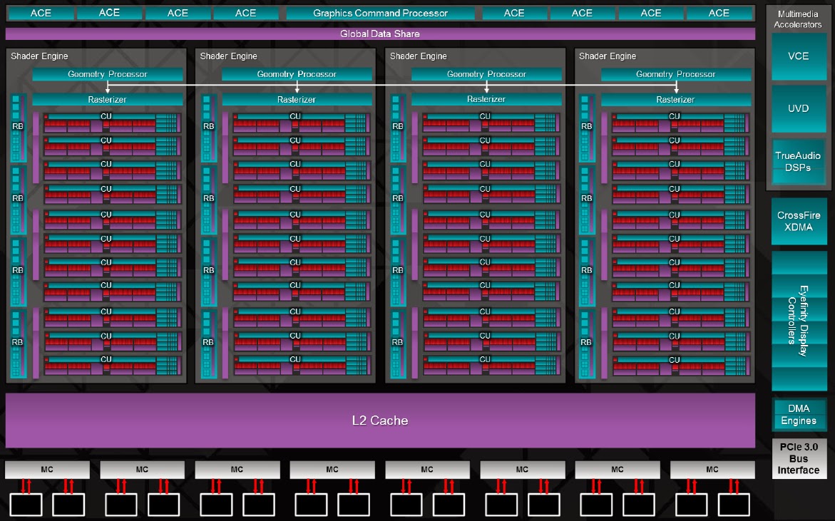
AMD GPU's already have Video Decoders\Encoders on the chip UVD & VCE

Maybe it's still a South bridge.

Last edited by a moderator:
There is no audio DSP. We've been told that, unless Sony have been lying.Edit: maybe it's the Audio DSP.
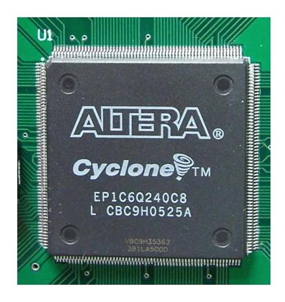
The PR blurb for the Altera Cyclone is as a replacement for costly, time-consuming ASICS. It could just be a supplementary chip pooling together all the other functions that'd be spread over other components. It's likely nothing exciting, or else we'd have been told about it (it's not an AI processor...).
AMD GPU's already have Video Decoders\Encoders on the chip UVD & VCE
Indeed - but the VCE latency is probably in the order of 16ms (just enough performance to record 1080P in more-or-less real time).
Using a hardware encoder would get that latency down to ~0ms, leaving only wifi/vita lag.
VCE is a hardware encoder.
VCE is a hardware encoder.
Doh! I know that, I just missed a few key words out
AFAICT VCE was originally designed for off-line compression/trans-coding - lately it's capable of 1080P@60, and it seems suitable for the 15m record feature.
But very low latency hardware encoders are capable of 1080p@60 compression into 2 streams at sub-1ms latency.
Basically, for 'remote play' Sony may have wanted to use a separate unit to get the lag down (and something similar is probably being installed into new "PS3" servers for Gaikai).
But it could just be a rather boring chip.
There is no audio DSP. We've been told that, unless Sony have been lying.
The PR blurb for the Altera Cyclone is as a replacement for costly, time-consuming ASICS. It could just be a supplementary chip pooling together all the other functions that'd be spread over other components. It's likely nothing exciting, or else we'd have been told about it (it's not an AI processor...).
Huh?


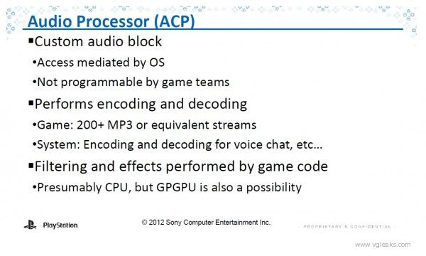
That's an audio decompressor and mixer, which isn't a DSP.Huh?

They talk about DSP (as a workload, not as a hardware component - Digital Signal Processing and not Digital Signal Processor) and then how it fits AMD's APU. Surely if PS4 had a DSP, they wouldn't be talking about audio processing on an HSA architecture?
To be fair, Shifty, it's perfectly possible they are using a DSP to accomplish the MP3 encoding/decoding and mixing.
- Status
- Not open for further replies.
Similar threads
- Replies
- 10
- Views
- 4K
- Replies
- 90
- Views
- 17K
- Replies
- 213
- Views
- 27K
- Replies
- 4
- Views
- 2K
